Faraday Delivers IP Solutions to Enable Endpoint AI Based on UMC's 28nm SST eFlash
Companies Mentioned
Why It Matters
The solution accelerates time‑to‑market for low‑power AI edge chips, a critical need as AIoT devices proliferate across industries. By delivering a ready‑made, silicon‑validated memory stack, Faraday helps designers cut development cycles and lower overall system cost.
Key Takeaways
- •Faraday's 28 nm SST‑ESF4 eFlash IP includes controller, BIST, and analog PHYs.
- •Integrated peripheral IPs improve test coverage, yield, and production ramp‑up.
- •Solution extends proven 55 nm SST experience to 28 nm with better performance.
- •Enables fast boot and low‑power AIoT edge SoCs, reducing development risk.
Pulse Analysis
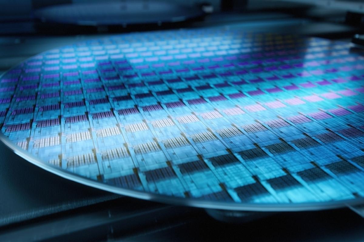
The surge in AI‑driven edge devices—from smart cameras to predictive maintenance sensors—has heightened demand for memory that can boot instantly while consuming minimal power. Traditional flash solutions often require extensive custom integration, adding time and risk to silicon projects. Faraday’s 28 nm SST‑ESF4 eFlash IP addresses this gap by delivering a turnkey memory subsystem that combines a flash controller, built‑in self‑test, and a portfolio of analog and high‑speed interfaces, all validated in silicon. This integration reduces the design‑to‑silicon timeline and offers a predictable performance envelope for AIoT SoCs.
Beyond the core flash block, Faraday bundles essential peripherals such as SRAM, USB, PLL, ADC/DAC, RTC, temperature sensors, oscillators, and generic I/O. By consolidating these functions into a single IP package, designers gain broader test coverage and higher manufacturing yields, as the IPs have been co‑optimized for timing and power across the 28 nm node. The end‑to‑end enablement—including characterization, verification kits, and test‑chip support—further de‑risks the path to volume production, a crucial advantage for startups and established fabless firms racing to ship AI‑enabled edge products.
Strategically, the move extends Faraday’s proven 55 nm SST expertise into the more advanced 28 nm process, delivering better speed and energy efficiency without sacrificing reliability. As enterprises push AI inference to the edge to reduce latency and bandwidth costs, a robust, low‑power non‑volatile memory solution becomes a differentiator. Faraday’s offering positions it as a key enabler for the next generation of AIoT and industrial edge platforms, potentially reshaping supply‑chain dynamics and accelerating adoption of intelligent edge workloads.
Faraday delivers IP solutions to enable endpoint AI based on UMC's 28nm SST eFlash
Comments
Want to join the conversation?
Loading comments...