New 'Serial' Tech Will Significantly Reduce the Cost of Memory — HBM Memory, that Is, the Sort of RAM only AI Hyperscalers Can Use, but Hey, at Least They Won't Go After Consumer RAM, or Would They?
•December 29, 2025
0
Companies Mentioned

Why It Matters
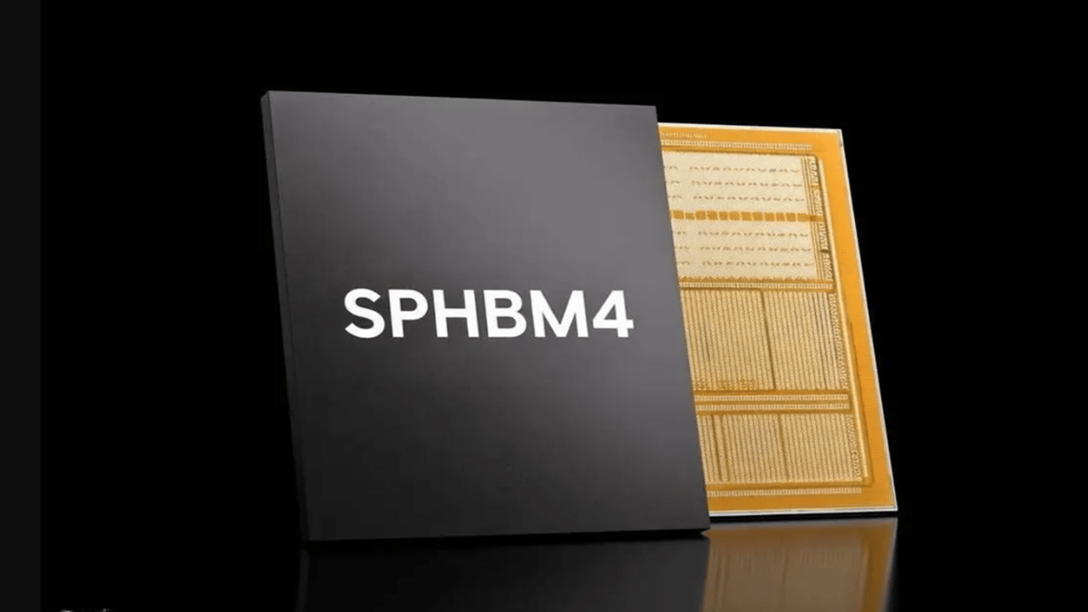
By cutting the most expensive part of HBM packaging, SPHBM4 can lower total cost of ownership for AI hyperscalers, accelerating adoption of high‑bandwidth memory in data‑center AI workloads.
Key Takeaways
- •SPHBM4 reduces pin count from 2048 to 512
- •4:1 serialization shifts complexity to signaling layer
- •Organic substrates replace silicon interposers, cutting costs
- •Maintains HBM-class bandwidth while lowering system cost
- •Targeted at AI hyperscalers, not consumer RAM
Pulse Analysis
High‑bandwidth memory (HBM) has become the backbone of AI accelerators and high‑performance computing, delivering terabytes‑per‑second data rates through ultra‑wide parallel interfaces. However, the traditional HBM architecture relies on thousands of pins and silicon interposers, driving up packaging complexity and cost. As AI models scale, data‑center operators face mounting pressure to balance performance with economics, making any reduction in the most expensive memory components a strategic priority.
The SPHBM4 proposal tackles these challenges by introducing 4:1 serialization, which compresses four physical pins into one high‑speed signaling lane. This architectural shift drops the pin count to 512 while operating at higher frequencies, preserving the aggregate bandwidth of HBM4. The lower pin density relaxes bump pitch requirements, allowing manufacturers to move from costly silicon interposers to organic substrates. Organic substrates are cheaper to produce, support larger channel lengths, and can accommodate more memory stacks per package, potentially boosting total capacity without sacrificing performance.
For hyperscale AI providers, the cost savings translate directly into lower total cost of ownership and higher revenue efficiency, as memory bandwidth remains a key determinant of accelerator throughput. Major JEDEC members such as Micron, Samsung, and SK Hynix are already investing in the standard, signaling industry alignment. While SPHBM4 will not democratize HBM for consumer PCs, its adoption could accelerate the rollout of larger, more affordable AI clusters, reinforcing the competitive edge of data‑center operators that can leverage cheaper, high‑bandwidth memory solutions.
New 'serial' tech will significantly reduce the cost of memory — HBM memory, that is, the sort of RAM only AI hyperscalers can use, but hey, at least they won't go after consumer RAM, or would they?
0
Comments
Want to join the conversation?
Loading comments...