
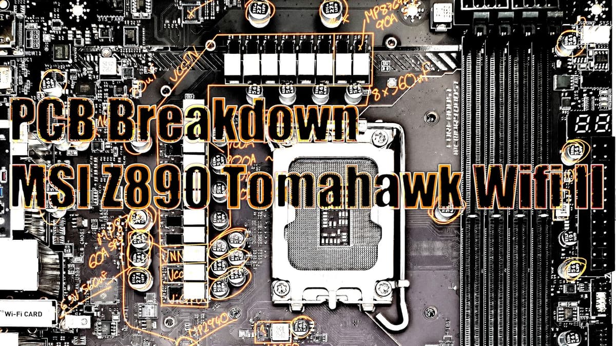
Mobo PCB Breakdown: MSI Z890 Tomahawk Wifi II
The video provides a detailed PCB walkthrough of MSI’s Z890 Tomahawk Wi‑Fi 2, highlighting its feature set and design choices for the latest Intel platform. Buildzoid examines the rear I/O panel, noting HDMI for iGPU output, a Thunderbolt‑compatible USB‑C, a second USB‑C, multiple USB‑A ports, 5 Gbps Killer LAN, Wi‑Fi 7, and a convenient clear‑CMOS button for BIOS resets without opening the case. Internally, the board offers a CPU‑direct Gen 5 M.2 slot, two Gen 4 M.2 slots on the CPU, and two chipset‑linked Gen 4 slots, while PCIe slots retain dedicated lanes—no sharing with M.2—allowing full simultaneous use and potential expansion via PCIe‑to‑M.2 adapters. However, MSI’s extra 8‑pin PCIe power connector is awkwardly placed under the bottom slot, rendering it unusable in triple‑GPU configurations, a recurring design quirk. Among the standout features, the Tomahawk includes a low‑cost post‑code display—rare on budget Z890 boards—providing granular boot diagnostics for overclockers. The clear‑CMOS button, dual 8‑pin CPU power connectors positioned near the PSU, and solid‑pin high‑current connectors improve usability and cable management. Power delivery relies on an MP2900 controller delivering eight effective phases with 16 smart stages, and a separate MP2940 for VNN, underscoring MSI’s over‑engineered approach. For system integrators, the board balances high‑end connectivity with practical design tweaks, making it a compelling choice for enthusiasts seeking Intel’s flagship chipset without premium pricing. The post‑code and improved power‑connector layout enhance troubleshooting and build ergonomics, while the misplaced extra PCIe power connector remains a caution for multi‑GPU users.
Ultra 7 270K and MSI Z890 Tomahawk Test/Bench Stream
The stream focuses on testing Intel’s Ultra 7 270K processor on an MSI Z890 Tomahawk motherboard, highlighting real‑world setup challenges and performance tweaks. The reviewer battles capture‑card artifacts that reappear after OS reinstalls, navigates missing BIOS options on Gigabyte boards, and experiments with...

Taking Power Rail Resistance Measurements of an RTX 5080
The video walks through a hands‑on investigation of an Inno3D RTX 5080, a stripped‑down, budget‑oriented variant that cannot adjust its power limit. Buildzoid bought the card on sale to compare its performance against his aging RX 970, only to discover the newer...

Gigabyte PLEASE FIX YOUR Z890 BIOS
Buildzoid’s video spotlights glaring omissions in Gigabyte’s Z890 BIOS, arguing that the board’s touted memory‑overclocking pedigree is undermined by absent settings. He notes that the BIOS lacks a power‑down mode off toggle, a feature present on competing ASRock, ASUS and...

Mobo PCB Breakdown: Asrock Z890 Taichi OCF
The video reviews ASRock's Z890 Taichi OC Formula motherboard, targeting extreme overclockers and test‑bench enthusiasts. Buildzoid walks through the rear I/O, highlighting a dual‑BIOS switch with an indicator LED, a clear CMOS button, and a BIOS flashback feature that updates...

RAMbling About DDR5 ODTs and Driver Strengths on Ryzen 9000
In this rambling tutorial, BuildSweet explains the purpose and function of DDR5 on‑die termination (ODT) and driver strength settings on AMD Ryzen 9000 platforms. He emphasizes that these parameters are electrical resistances measured in ohms, not memory timing values, and...
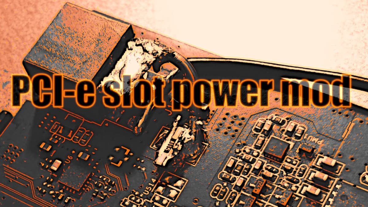
Converting an ASUS GTX 950 Strix to Run on only PCI-E Slot Power.
YouTuber BuildZoid documents a hardware mod converting an ASUS GTX 950 Strix to run solely from the PCIe slot by raising the shunt resistor for the auxiliary 6‑pin feed and rewiring the card so the 6‑pin, when plugged in, bypasses...

Testing Ryzen DDR5 Refresh Modes with Dual Rank Hynix 24Gb M-Die
The video examines how the new DDR5 refresh‑mode options on AMD’s AM5 platform affect performance with a dual‑rank 24 Gb Hynix M‑die kit (Corsair 2 × 48 GB 6000 CL30). Using an ASUS Crosshair X870 Hero with BIOS 20004 (AGSA 1.3.0.0.0), Buildzoid compares the standard "normal" mode, the...
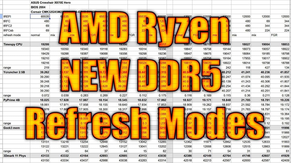
New DDR5 Refresh Modes on AM5 Motherboards
AMD AM5 motherboards from ASUS and Gigabyte now expose a Bank Refresh Mode setting that lets users choose between legacy (all-bank) refresh, fine-granularity refresh (FGR), and a mixed mode that switches dynamically. FGR refreshes one bank per bank group instead...