Enphase Explains How Gallium Nitride Is Changing Its Microinverters
Why It Matters
GaN‑based inverters promise lower cost, higher efficiency and smaller form factors, reshaping commercial solar, EV‑charging and data‑center power markets. The shift gives Enphase a competitive edge as the industry seeks higher power density and reliability.
Key Takeaways
- •GaN BDS reduces die area fourfold versus silicon back‑to‑back designs
- •Higher switching frequencies shrink passive components and heat‑sink requirements
- •Enphase’s roadmap targets IQ10 inverters, EV chargers and AI data‑center modules
- •GaN’s over‑voltage and radiation resilience cuts external protection costs
Pulse Analysis
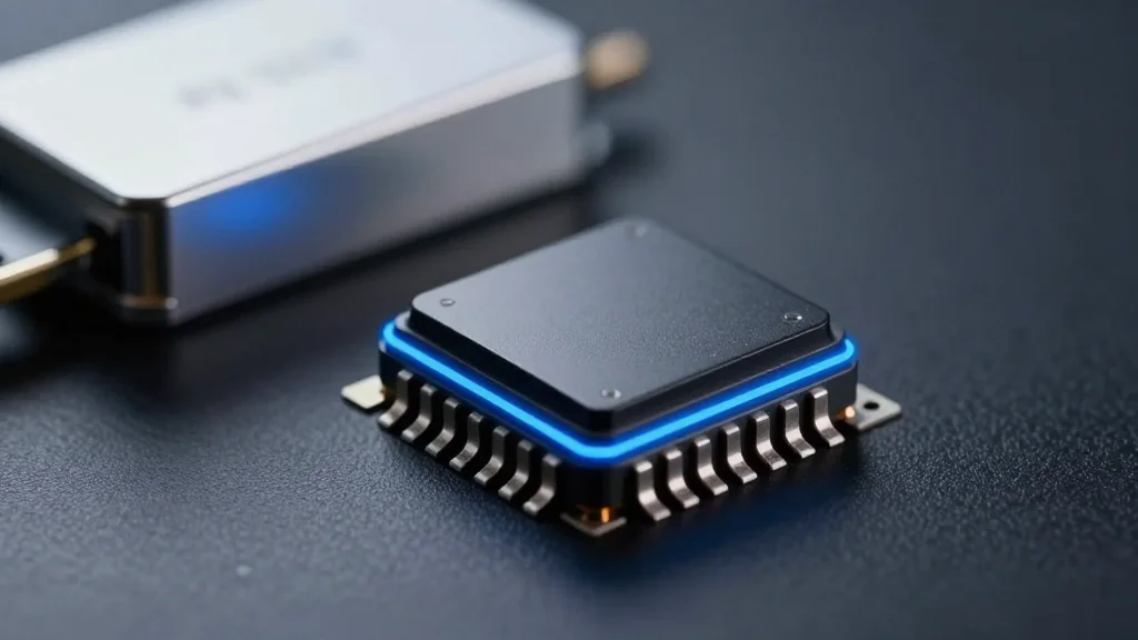
Gallium‑nitride is rapidly emerging as the preferred semiconductor for high‑performance power conversion, and Enphase’s latest white paper underscores why. By moving from silicon MOSFETs to a monolithic GaN bidirectional switch, the company eliminates the bulk of traditional back‑to‑back transistor stacks. This architectural shift not only trims die size by roughly ten times but also slashes conduction losses, allowing switching frequencies to climb into the megahertz range. The result is a dramatic reduction in inductors, capacitors and heat‑sink mass, which translates into lighter, more compact inverters that can be deployed in tighter spaces.
From a technical standpoint, GaN’s wide bandgap delivers superior over‑voltage tolerance and resistance to single‑event burnout, issues that have long plagued silicon devices in grid‑connected applications. Enphase leverages these attributes to simplify surge‑protection circuitry and improve long‑term reliability, especially in harsh environments like solar farms and data‑center racks. The integrated substrate‑management circuit embedded on‑die ensures the GaN BDS remains correctly biased, mitigating the risk of back‑gate conduction and further enhancing device robustness. These benefits collectively lower the bill of materials while boosting efficiency beyond the 97% threshold already demonstrated in the IQ9N‑3P series.
Commercially, the move positions Enphase at the forefront of a broader industry transition toward all‑GaN power architectures. The company’s plan to roll the technology into IQ10 microinverters, bi‑directional EV chargers and the IQ SST modules for AI data centers signals a strategic push into high‑growth segments that demand both power density and reliability. As manufacturing scales and GaN costs continue to fall, Enphase can pass savings to customers, accelerating adoption across residential, commercial and industrial markets. Analysts see this as a catalyst for faster market penetration of next‑generation solar and storage solutions, potentially reshaping the competitive landscape for inverter manufacturers worldwide.
Enphase explains how gallium nitride is changing its microinverters
Comments
Want to join the conversation?
Loading comments...