SOSV Deep Tech Live – The Atomic Architect: Rick Gottscho on Plasma’s Role in Semiconductor Fabrication & Physical AI Infrastructure
Companies Mentioned
Why It Matters
Plasma‑based manufacturing offers a viable route to continue transistor scaling and satisfy exploding AI compute needs, crucial for maintaining competitiveness in the semiconductor supply chain.
Key Takeaways
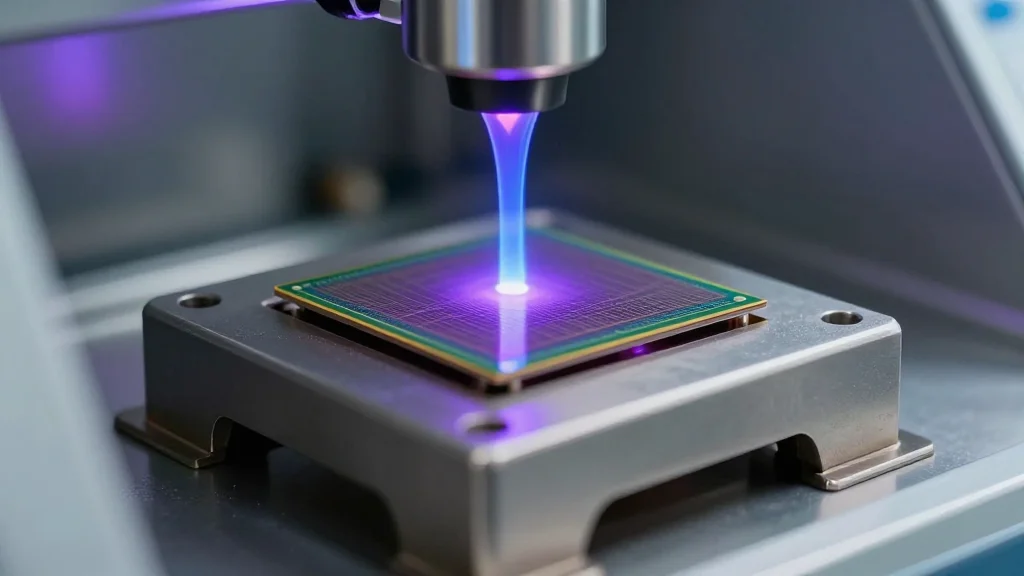
- •Plasma etching enables sub‑nanometer transistor scaling beyond Moore's Law
- •AI workloads drive unprecedented precision in wafer fabrication processes
- •Rick Gottscho shares strategies for moving lab plasma tech to mass production
- •Event highlights reshoring semiconductor manufacturing for supply‑chain resilience
- •SOSV Deep Tech Live offers networking for founders in physical AI sector
Pulse Analysis
The semiconductor industry stands at a crossroads as traditional silicon scaling approaches the physical limits that once underpinned Moore's Law. Engineers are turning to plasma‑based processes—such as reactive ion etching and atomic layer deposition—to achieve sub‑nanometer feature sizes and novel material integrations. These techniques provide the fine‑grained control needed for next‑generation transistors, enabling performance gains without relying on sheer transistor count. As AI models demand ever‑greater compute power, the precision and throughput of plasma tools become strategic assets for chipmakers.
Beyond the fab floor, plasma technology is influencing the broader physical AI infrastructure. Advanced packaging, 3D‑stacked dies, and heterogeneous integration all depend on high‑quality plasma treatments to ensure reliable interconnects and thermal management. This convergence means that AI hardware designers must consider plasma capabilities when architecting systems, aligning device physics with algorithmic requirements. Companies that master plasma‑enabled manufacturing can deliver chips that meet AI workloads while reducing power consumption—a critical differentiator in a market where efficiency drives profitability.
The upcoming SOSV Deep Tech Live fireside chat offers a rare platform for industry insiders and startup founders to glean insights from Rick Gottscho, a veteran of Lam Research's plasma innovations. His perspective on translating laboratory breakthroughs into scalable production lines, coupled with discussions on reshoring and supply‑chain resilience, equips participants with actionable knowledge. For entrepreneurs building physical AI solutions, the event provides networking opportunities and a glimpse into the evolving ecosystem that will define the next era of semiconductor technology.
SOSV Deep Tech Live – The Atomic Architect: Rick Gottscho on Plasma’s Role in Semiconductor Fabrication & Physical AI Infrastructure
Comments
Want to join the conversation?
Loading comments...