A Materials Scientist’s Playground
Why It Matters
The MBE gives researchers atomic‑scale control and in‑situ interface analysis, speeding the material breakthroughs needed for scalable, low‑error quantum computers and strengthening U.S. quantum leadership.
Key Takeaways
- •MIT.nano hosts the US’s largest 1‑meter MBE deposition chamber.
- •Six‑chamber design includes in‑vacuum XPS for buried‑interface analysis.
- •System enables atomic‑scale growth of superconducting and ceramic qubit films.
- •Installation completed in under three weeks thanks to CHIPS‑Act‑ready infrastructure.
- •ARO and LPS grants fund the tool, supporting national‑security quantum research.
Pulse Analysis
Quantum computers promise exponential speedups, yet qubit coherence is limited by material defects and environmental noise. Circuit‑level tweaks have yielded diminishing returns, shifting focus to the underlying materials that host superconducting qubits. Molecular beam epitaxy (MBE) provides atomic‑scale control, enabling deposition of ultra‑pure superconducting metals and dielectric layers one atom at a time. Precise control of stoichiometry, crystallinity, and interface chemistry can suppress two‑level system defects that currently cap qubit lifetimes. MIT.nano’s new MBE system thus tackles the materials bottleneck essential for scalable quantum processors.
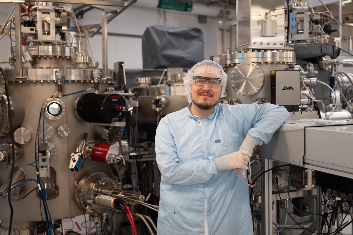
The MIT‑nano platform houses a six‑chamber, 200‑mm wafer MBE occupying 600 sq ft, with the nation’s largest single‑deposition chamber (1 m diameter). In addition to growth, the system includes an oxidation module, a ten‑wafer storage vault, and a unique X‑ray photoelectron spectroscopy (XPS) chamber that probes buried interfaces without breaking vacuum. This in‑situ analysis lets researchers monitor chemical states layer by layer, cutting feedback cycles dramatically. Integrated into MIT.nano’s ultra‑stable cleanroom, the tool benefits from sub‑ppm particle counts and tightly regulated humidity, ensuring repeatable, high‑yield qubit fabrication.
Funding from the Army Research Office’s Defense University Research Instrumentation program and MIT’s Laboratory for Physical Sciences ties the MBE to national‑security goals, reinforcing U.S. quantum leadership. The three‑week commissioning—accelerated by prior CHIPS Act infrastructure upgrades—shows how coordinated campus planning can fast‑track capital‑intensive equipment. As MIT’s Quantum Initiative expands, the MBE will bridge materials science and device engineering, improving interface quality and boosting qubit yield. Ultimately, lower‑defect films could reduce production costs and bring fault‑tolerant quantum computers nearer to commercial deployment.
A materials scientist’s playground
Comments
Want to join the conversation?
Loading comments...