Fermilab and MIT Lincoln Laboratory Demonstrate Cryoelectronic Control of Ion-Trap Qubits
Key Takeaways
- •Cryoelectronic ASIC controlled ion movement inside vacuum
- •Low‑power chips reduced thermal noise, improved sensitivity
- •Demonstration supports scaling ion traps to thousands of qubits
- •Transistor behavior varied at deeper cryogenic temperatures
- •Voltage hold times need extension for long‑duration operations
Pulse Analysis
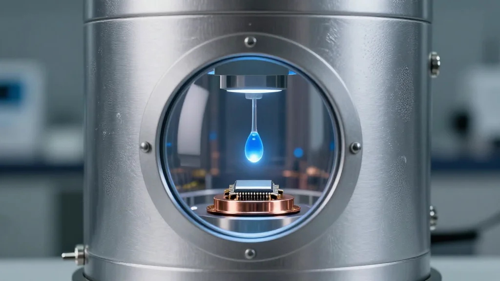
Ion‑trap quantum computers have long been prized for their exceptional coherence times, yet scaling them beyond a few hundred qubits has been hampered by bulky room‑temperature control hardware and extensive wiring that introduce thermal noise and latency. Traditional architectures route laser‑driven operations and voltage signals from ambient electronics through cryogenic stages, a scheme that becomes impractical as qubit counts rise into the thousands. Embedding control electronics within the cryogenic environment promises to shrink the footprint, lower power consumption, and dramatically improve signal fidelity, positioning ion traps as a viable contender for large‑scale quantum processors.
The recent Fermilab‑MIT Lincoln Laboratory demonstration marks a concrete step toward that vision. By integrating a compact, application‑specific integrated circuit (ASIC) that operates at millikelvin temperatures directly onto the ion‑trap platform, the team showed reliable ion transport, precise positioning, and measurable reductions in electronic noise. This hybrid approach, enabled through the DOE Quantum Science Center and Quantum Systems Accelerator, validates the feasibility of cryoelectronic control while surfacing practical challenges: certain transistors underperformed at the deeper cryogenic temperatures of the MIT setup, and voltage‑hold durations, initially measured in milliseconds, must be extended to minutes or hours for real‑world workloads. Addressing these issues will be critical for moving from proof‑of‑concept to production‑grade hardware.
Looking ahead, the successful integration signals a shift in quantum hardware roadmaps, encouraging investment in cryogenic microelectronics and cross‑institutional collaborations. As the industry seeks fault‑tolerant quantum advantage, the ability to densely pack tens of thousands of low‑noise electrodes could unlock new algorithmic capabilities in chemistry, materials science, and optimization. Continued development of robust cryoelectronic components, alongside advances in ion‑trap chip design, will likely accelerate commercialization timelines, positioning the United States at the forefront of scalable quantum computing technology.
Fermilab and MIT Lincoln Laboratory Demonstrate Cryoelectronic Control of Ion-Trap Qubits
Comments
Want to join the conversation?