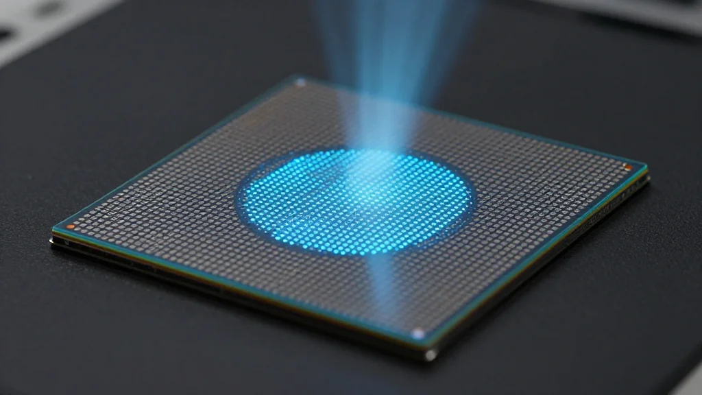
Imec Unveils First 6 Nm Quantum Dot Qubit Chip, Paving Way for Scalable Processors

Companies Mentioned
Why It Matters
The ability to fabricate quantum dot qubits with 6 nm gate spacing using a standard 300 mm wafer process could fundamentally change the economics of quantum computing. By leveraging existing semiconductor infrastructure, the breakthrough reduces the need for bespoke, low‑volume manufacturing, making quantum chips more affordable and accelerating their deployment in real‑world applications such as cryptography, materials science, and complex optimization. Moreover, the demonstration validates High NA EUV lithography as a viable tool for quantum hardware, potentially aligning the quantum and classical semiconductor roadmaps and fostering cross‑industry collaboration. Beyond cost, the tighter gate spacing improves qubit control fidelity, a key metric for error‑corrected quantum computing. Higher fidelity translates to lower error rates, bringing fault‑tolerant architectures closer to feasibility. As governments and investors prioritize scalable quantum solutions, Imec’s achievement could attract new funding, stimulate partnerships with major foundries, and influence policy decisions around quantum manufacturing capabilities.
Key Takeaways
- •Imec built a quantum dot qubit array with 6 nm gate spacing using High NA EUV lithography.
- •The chip is fabricated on a 300 mm wafer, compatible with mainstream semiconductor fabs.
- •Silicon quantum dot qubits leverage existing manufacturing lines, enabling potential mass production.
- •The breakthrough could shorten the timeline for commercial quantum computers from the projected 2030 target.
- •Imec plans to collaborate with major foundries to scale the technology, though details remain undisclosed.
Pulse Analysis
Imec’s 6 nm quantum chip is more than a laboratory curiosity; it signals a convergence of two historically divergent technology streams—classical semiconductor manufacturing and quantum hardware. Historically, quantum research has been hamstrung by the lack of a scalable, cost‑effective production method. By co‑opting High NA EUV lithography, a tool that underpins the latest logic nodes for chips like Apple’s A‑series processors, Imec effectively bridges that gap. This could trigger a wave of investment into silicon‑based quantum platforms, which have previously been viewed as less exotic but more pragmatic than superconducting or ion‑trap approaches.
The competitive advantage lies in supply chain readiness. Foundries such as TSMC, Samsung, and GlobalFoundries already operate 300 mm lines capable of High NA EUV. If Imec can certify a quantum‑ready process flow, these fabs could start offering quantum‑grade silicon wafers alongside traditional products, creating a new revenue stream and diversifying their portfolios. This would also force other qubit technologies to justify higher costs or demonstrate superior performance, potentially reshaping R&D priorities across the sector.
Looking ahead, the critical hurdle will be moving from a functional prototype to a production‑ready design with error rates low enough for error‑corrected computing. Imec’s next milestones—larger qubit arrays, integration with cryogenic control electronics, and partnership announcements—will determine whether the promise of a silicon‑based quantum ecosystem materializes. If successful, the industry could see a shift from niche, lab‑scale quantum processors to commercially viable chips that can be manufactured in the same fabs that produce today’s smartphones, fundamentally altering the quantum computing value chain.
Imec Unveils First 6 nm Quantum Dot Qubit Chip, Paving Way for Scalable Processors
Comments
Want to join the conversation?
Loading comments...