Japanese Researchers Pinpoint Charge Noise Source, Boost Silicon Qubit Stability
Companies Mentioned
Why It Matters
The identification of charge‑noise origins directly addresses the decoherence bottleneck that has limited silicon qubits from scaling to fault‑tolerant sizes. By providing a concrete, temperature‑dependent model, the research enables engineers to design chips that operate at higher temperatures, lowering cryogenic costs and simplifying system integration. This could shift the balance of power toward silicon‑based platforms, which already benefit from mature semiconductor manufacturing, and accelerate the timeline for quantum‑enhanced computing in fields like cryptography, materials science, and optimization. Furthermore, the breakthrough narrows the gap between academic research and commercial production. With a clear engineering roadmap, venture capital and corporate R&D can allocate resources more efficiently, reducing the risk associated with speculative hardware development. The ripple effect may also stimulate ancillary markets—cryogenic infrastructure, control electronics, and software stacks—creating a broader quantum ecosystem anchored in silicon technology.
Key Takeaways
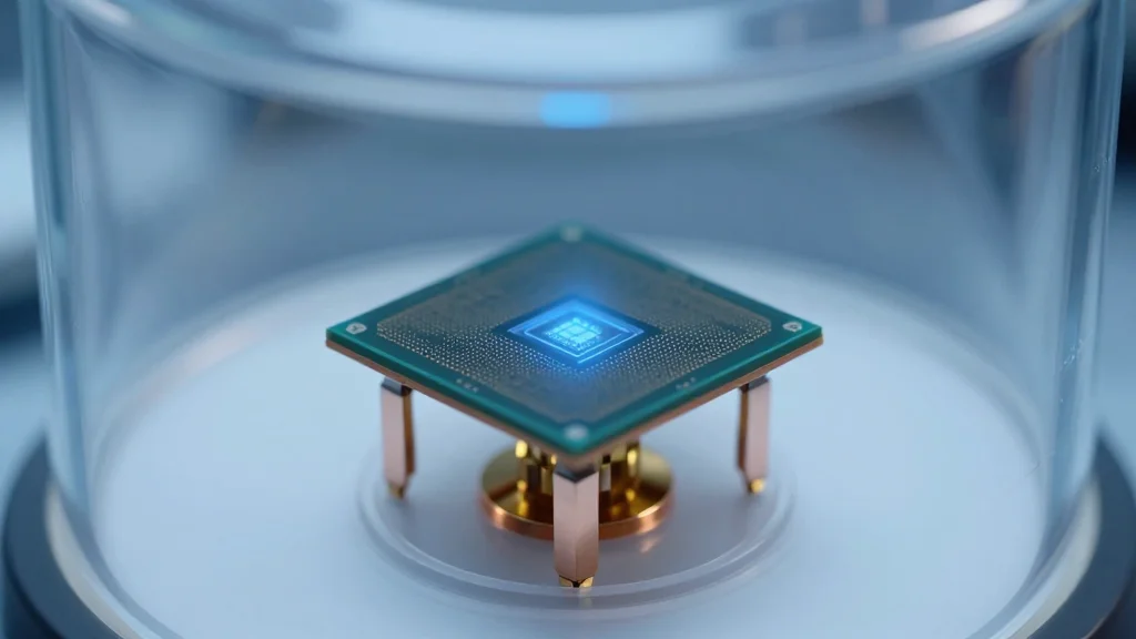
- •Japanese team identifies two‑level fluctuators as the primary source of charge noise in silicon spin qubits.
- •Raising qubit temperature from 20 mK to 200 mK reduces frequency drift and improves gate fidelity.
- •Mathematical blueprint released for designing noise‑resilient silicon quantum processors.
- •Potential to lower cooling costs and accelerate fab‑compatible quantum chip production.
- •Industry analysts see the breakthrough as a catalyst for increased investment in silicon‑based quantum hardware.
Pulse Analysis
The discovery that modest temperature increases can suppress charge noise flips a long‑standing assumption that colder is always better for quantum coherence. Historically, silicon qubit research has been hamstrung by the need to operate at sub‑20 mK temperatures, driving up system complexity and cost. By demonstrating a clear physical mechanism—TLFs whose switching rates diminish at higher temperatures—the Japanese study offers a pragmatic lever for engineers. This could usher in a new generation of silicon chips that run at 200 mK, a regime already accessible to commercial dilution refrigerators, thereby narrowing the cost gap with classical semiconductor fabs.
From a market perspective, the timing aligns with a surge of capital flowing into silicon‑based quantum startups. The blueprint reduces technical uncertainty, which should translate into tighter development cycles and earlier product rollouts. Companies that can quickly integrate the model into their design pipelines stand to capture early market share, especially in sectors where cost‑effective quantum acceleration is critical, such as finance and logistics. Conversely, superconducting players may need to double down on performance metrics to justify their higher cooling overhead, potentially leading to a more segmented quantum hardware landscape.
Looking forward, the real test will be the upcoming prototype chip that incorporates the TLF‑mitigation design. If it validates the simulation results, we could see a cascade of fab‑scale production orders within the next 12‑18 months. That would not only accelerate the path to error‑corrected logical qubits but also create a virtuous cycle: more silicon chips lead to more data, refining the noise models further, and driving iterative improvements. In short, the study provides both a scientific breakthrough and a strategic inflection point for the quantum hardware industry.
Japanese Researchers Pinpoint Charge Noise Source, Boost Silicon Qubit Stability
Comments
Want to join the conversation?
Loading comments...