Microscopic Mirrors for Future Quantum Networks: A New Way to Make High-Performance Optical Resonators
•February 18, 2026
0
Why It Matters
The method delivers ultra‑low‑loss, mass‑producible photonic interfaces essential for scaling quantum computers and integrated optical systems, accelerating industry adoption.
Key Takeaways
- •Record 0.9‑million finesse at 780 nm
- •Mirrors fabricated via stress‑buckling on silicon
- •Process yields tunable curvature and wavelength response
- •Scalable method suitable for chip‑integrated photonics
- •Improves photon‑atom coupling for quantum networks
Pulse Analysis
Optical resonators are the backbone of modern photonic devices, from atomic clocks to data‑center lasers. Traditional lithography often leaves surface roughness that scatters light, limiting cavity finesse and, consequently, the efficiency of photon‑atom interactions. As quantum technologies demand ever‑smaller, low‑loss cavities, researchers have been forced to balance precision with manufacturability, a trade‑off that has slowed the rollout of scalable quantum hardware.
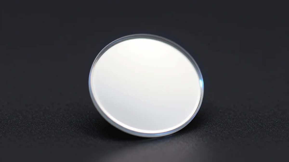
The Harvard team sidestepped these constraints by exploiting material stress rather than aggressive etching. After growing a thin silicon‑oxide layer to smooth the wafer, they removed it, deposited a dielectric stack, and allowed intrinsic stress to buckle the film into a perfect curvature. This simple, repeatable process lets engineers dial in radius of curvature and target wavelength, achieving a record‑breaking finesse of 0.9 million at 780 nm. Such performance rivals the best macroscopic cavities while occupying a footprint measured in tens of micrometers.
Beyond quantum networking, the technique opens doors for ultra‑compact lasers, on‑chip spectroscopic sensors, and dense photonic interconnects. Its scalability aligns with semiconductor‑foundry workflows, promising lower production costs and faster time‑to‑market for next‑generation photonic chips. As the industry pushes toward modular quantum processors and integrated photonic circuits, these microscopic mirrors could become the standard interface that bridges atoms, photons, and silicon.
Microscopic mirrors for future quantum networks: A new way to make high-performance optical resonators
0
Comments
Want to join the conversation?
Loading comments...