New Approach to Circuit Design Introduces Next-Level Quantum Computing
•January 27, 2026
0
Why It Matters
Efficient multi‑wavelength laser delivery is essential for scaling trapped‑ion quantum processors, and this approach directly tackles that hardware limitation. It opens a pathway toward larger, more practical quantum computers and versatile photonic devices.
Key Takeaways
- •Nanophotonic circuit routes six laser wavelengths efficiently.
- •Waveguide design enables independent on/off control of beams.
- •Approach could scale to several hundred qubits per chip.
- •Bubble sort and blockwise duplication patterns optimize loss trade‑offs.
- •Technique applicable to broader advanced optical systems.
Pulse Analysis
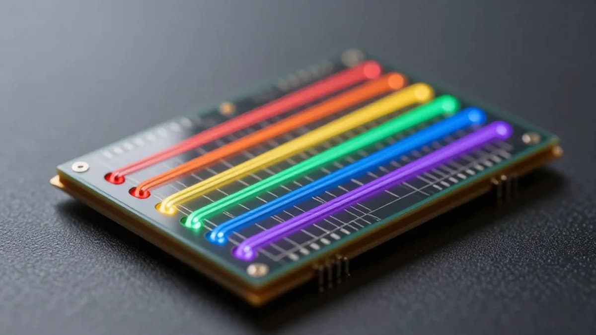
Trapped‑ion quantum computers rely on precisely timed laser pulses to manipulate individual ions, but delivering dozens of wavelengths within a cramped vacuum chamber has long been a logistical nightmare. Conventional free‑space optics demand bulky mirrors and alignment rigs, which limit chip density and increase thermal load. By embedding the light‑routing function directly onto a photonic chip, engineers can shrink the optical footprint, reduce alignment drift, and improve overall system stability—critical factors for moving quantum hardware from the lab to commercial environments.
The Osaka team’s solution integrates six separate laser channels into a single nanophotonic platform using silicon‑based waveguides coupled to optical fibers. Their routing algorithms—dubbed bubble sort and blockwise duplication—organize the waveguide network to minimize crosstalk and insertion loss while allowing each beam to be switched on or off independently. This modularity not only preserves power efficiency but also simplifies control electronics, enabling rapid reconfiguration of trapping zones. The resulting layout resembles an intricate tapestry, yet each strand is engineered for optimal transmission, demonstrating that complex photonic architectures can be both functional and manufacturable.
Beyond immediate quantum‑computing gains, the technology promises to accelerate the development of high‑bandwidth optical interconnects, on‑chip spectroscopy, and lidar systems that require multi‑color light delivery. Scaling the waveguide approach could accommodate hundreds of qubits, pushing trapped‑ion platforms toward fault‑tolerant thresholds. As the semiconductor industry embraces photonic integration, such cross‑disciplinary innovations are poised to reshape both quantum information processing and broader photonics markets, offering a compelling value proposition for investors and technology adopters alike.
New approach to circuit design introduces next-level quantum computing
0
Comments
Want to join the conversation?
Loading comments...