Sony and TSMC Launch AI‑focused Image Sensor JV in Kumamoto
Companies Mentioned
Why It Matters
The Sony‑TSMC joint venture marks a pivotal moment for hardware‑centric AI development. By embedding neural processing directly into image sensors, the partnership addresses latency and power constraints that have limited edge AI adoption. CTOs across sectors—from automotive to retail—will need to reconsider system architectures, potentially reducing reliance on central GPUs and shifting budgets toward sensor‑level intelligence. Moreover, the alliance strengthens Japan’s semiconductor ecosystem, offering a counterbalance to the concentration of advanced manufacturing in Taiwan and South Korea. If successful, AI‑enabled sensors could accelerate the rollout of autonomous systems, improve real‑time analytics in factories, and enable new consumer experiences such as ultra‑responsive AR glasses. The venture also illustrates how component vendors are moving beyond traditional supply relationships to co‑develop differentiated technology, a pattern likely to repeat as AI workloads become more specialised.
Key Takeaways
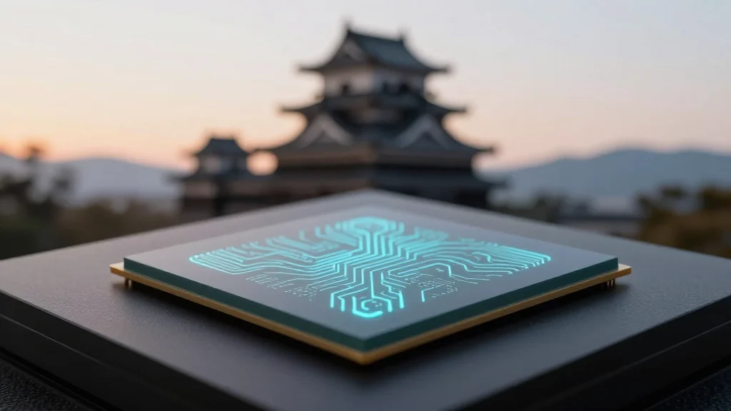
- •Sony Semiconductor Solutions and TSMC announce a joint venture in Kumamoto to develop AI‑focused image sensors.
- •The partnership will leverage TSMC’s 3‑nm process node, with production targeted for late 2027.
- •Joint R&D will embed AI inference engines directly on sensor chips, cutting latency and power use.
- •Both firms will share IP ownership and split development costs, aiming for first patents by mid‑2026.
- •Prototype chips are planned for CES 2027, offering a tangible benchmark for CTOs evaluating edge AI solutions.
Pulse Analysis
The Sony‑TSMC alliance reflects a strategic pivot from generic silicon supply to purpose‑built AI hardware. Historically, image sensors have been passive converters; now they are evolving into active processors capable of recognizing objects, gestures and anomalies without external compute. This evolution mirrors the broader trend of heterogeneous integration, where specialized accelerators are co‑located with sensors, memory and networking to form ultra‑compact AI modules.
From a market perspective, the joint venture could reshape competitive dynamics. Samsung and Qualcomm have pursued AI at the SoC level, but integrating AI into the sensor itself offers a unique value proposition: reduced data movement and lower system cost. If Sony and TSMC can deliver a cost‑effective solution, they may capture a sizable share of the projected $30 billion AI‑enabled imaging market by 2030. However, the venture must navigate the tight capacity constraints at TSMC’s most advanced nodes, where demand from smartphones, high‑performance computing and automotive chips already strains supply.
For CTOs, the emergence of AI sensors introduces new decision points. System architects will need to evaluate trade‑offs between on‑sensor processing versus centralized AI pipelines, factoring in latency, power budgets, and security considerations. The partnership also underscores the importance of cross‑industry collaboration; hardware leaders are no longer isolated silos but co‑creators of end‑to‑end AI solutions. As the joint venture matures, we can expect a cascade of downstream innovations—smart cameras with built‑in threat detection, autonomous drones that process visual data in‑flight, and AR devices that render scenes with millisecond response times. The next few years will reveal whether this hardware‑first approach can outpace software‑centric AI strategies and become the new standard for edge intelligence.
Sony and TSMC launch AI‑focused image sensor JV in Kumamoto
Comments
Want to join the conversation?
Loading comments...