
Researchers “Reprogram” Materials by Quickly Rearranging Their Atoms
A collaborative team from MIT, Oak Ridge National Laboratory and partners has unveiled a room‑temperature electron‑beam technique that can reposition tens of thousands of individual atoms within a solid in minutes. By deploying custom algorithms to steer the beam with picometer precision, the researchers created over 40,000 quantum defects in a chromium‑based semiconductor in roughly 40 minutes. The method works in three dimensions, bypassing the surface‑only constraints of earlier scanning‑probe approaches. This scalable, fast atomic‑reprogramming opens a new route to engineered quantum materials.

Improving the Reliability of Circuits for Quantum Computers
MIT and Lincoln Laboratory have unveiled a new method to detect and quantify second-order harmonic corrections that cause two‑Cooper‑pair tunneling in superconducting quantum circuits. By fabricating a test device that suppresses single‑pair tunneling while allowing the double‑pair process, the team...
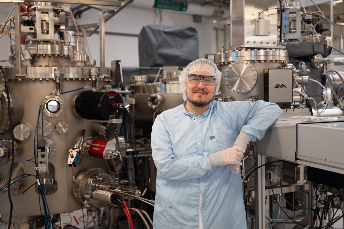
A Materials Scientist’s Playground
MIT.nano has installed a custom 200‑mm wafer molecular beam epitaxy (MBE) system, the largest single‑deposition chamber sold in the United States. The six‑chamber tool enables in‑vacuum growth, oxidation, storage and X‑ray photoelectron spectroscopy (XPS) for real‑time analysis of superconducting and...

The MIT-IBM Computing Research Lab Launches to Shape the Future of AI and Quantum Computing
MIT and IBM have launched the MIT‑IBM Computing Research Lab, expanding the former Watson AI Lab to include quantum computing. The new three‑focus‑area lab—AI, algorithms, and quantum—will develop hybrid AI‑quantum systems, advance foundational mathematics, and train the next generation of...

New Chip Can Protect Wireless Biomedical Devices From Quantum Attacks
MIT engineers have unveiled a needle‑tip ASIC that brings post‑quantum cryptography to wireless biomedical implants such as pacemakers and insulin pumps. The chip achieves 20‑60× higher energy efficiency than existing PQC implementations while adding on‑chip random number generation, side‑channel protection...

Sixteen New START.nano Companies Are Developing Hard-Tech Solutions with the Support of MIT.nano
MIT.nano announced that 16 hard‑tech startups joined its START.nano accelerator in 2025, more than doubling the previous year’s intake. The program offers discounted access to MIT.nano’s shared facilities and a gateway to the institute’s broader innovation network. Cohort companies are...
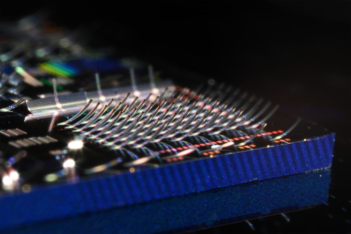
New Photonic Device Efficiently Beams Light Into Free Space
Researchers at MIT, MITRE, Sandia and the University of Arizona have unveiled a photonic chip that uses upward‑curving “ski‑jump” structures to broadcast thousands of individually controllable laser beams into free space. The device leverages a bimaterial strain technique—silicon nitride and...

Efficient Cooling Method Could Enable Chip-Based Trapped-Ion Quantum Computers
MIT and MIT Lincoln Laboratory have demonstrated a photonic‑chip based cooling technique that reduces trapped‑ion temperatures to roughly ten times below the conventional Doppler limit. The method uses polarization‑gradient cooling generated by nanoscale antennas on the chip, achieving the cooling...

Anything-Goes “Anyons” May Be at the Root of Surprising Quantum Experiments
MIT theorists propose that electrons in certain two‑dimensional materials can fractionalize into anyons, allowing superconductivity to coexist with magnetism. Their calculations show that when 2/3‑charge anyons dominate, they overcome quantum frustration and form a frictionless supercurrent, unlike conventional Cooper‑pair superconductors....