
Different Types of Registers in Processor Architecture Explained ||RISC - V Processor Design || ABV
The video walks viewers through the core registers that underpin a RISC‑V processor, framing the discussion as part of a broader VLSI design series. It outlines each register’s purpose—addressing, data movement, instruction sequencing, and I/O handling—while tying them to the underlying bus architecture. Key insights include the interplay between the Memory Address Register (MAR) and Memory Data Register (MDR): MAR places the target address on the address bus, and MDR carries the actual data on the data bus. The Program Counter (PC) automatically increments to fetch the next instruction, while the accumulator serves as the primary scratch pad for ALU results. Additional registers such as the Instruction Register, Interrupt Register, and Output Register orchestrate control flow and external communication. The presenter illustrates concepts with concrete examples, loading address 002 into MAR to read data, and showing PC value 004 driving the next fetch. He also quantifies addressable memory: 16‑bit MAR yields 64 KB, 20‑bit yields 1 MB, and 32‑bit reaches 4 GB, underscoring the scalability of register width. Understanding these registers is vital for architects designing efficient RISC‑V cores, as they dictate how instructions are fetched, executed, and how data moves between CPU and memory. Mastery of this register set enables more effective debugging, performance tuning, and custom processor extensions.
Introduction to Processors | Fetch - Decode - Execute | All About VLSI || RISC - V Processor Design
The video introduces the three core stages of processor operation—fetch, decode, and execute—to lay a foundation for learning RISC‑V CPU design. It targets VLSI beginners, FPGA hobbyists, and computer‑architecture students, emphasizing that mastering these cycles simplifies later work with RISC‑V...
MII Interface Explained in Ethernet | MAC to PHY Communication || All About VLSI ||
The video introduces the Media Independent Interface (MII) as the standard link between an Ethernet MAC controller and a PHY chip, highlighting its role in separating digital frame handling from analog signal conversion. It outlines the overall Ethernet stack covered...
SystemVerilog Testbench Day 12 | Top Module Design | Connecting DUT & Verification Environment
The video walks through building the top‑level SystemVerilog testbench for a decoder‑based RAM verification project. It shows how the top module creates a clock, instantiates the RAM design, the verification interface, and a test class handle, then uses $value$plusargs to...
Barrel Shifter Design in Verilog | High Speed Shifter Architecture | Verilog Project Series
The video walks through a Verilog implementation of a barrel shifter, a high‑speed combinational circuit that can rotate or shift a data word left or right by any number of bits in a single clock cycle. It builds on earlier...
FSM Sequence Detector 101 Design with Clock Gating | Verilog Project Development Series
The video walks through a Verilog implementation of a 101 sequence detector that incorporates clock gating to reduce dynamic power consumption. After a brief recap of prior projects, the presenter explains that clock gating selectively disables the clock for portions...
SystemVerilog Testbench Day 11 | Test Case Development for Decoder RAM
The video walks through a SystemVerilog testbench for a decoder‑based RAM, detailing how to construct and extend test cases within a UVM‑style environment. Fifteen distinct test scenarios are described, ranging from a random test (32 writes, 16 reads) and block‑boundary checks...

CRC in Ethernet Frames | Error Detection Explained || Ethernet MAC Controller Design Series || ABV||
The video explains how Ethernet frames use a 32‑bit Frame Check Sequence (FCS) based on cyclic redundancy check (CRC) to detect transmission errors. It is part of a series on MAC controller design, focusing on the CRC32 algorithm that appends...
SRAM Verilog Code Implementation | 6T SRAM Design in Verilog | VLSI Project Series
The video walks through a Verilog implementation of a simple 6T SRAM controller, detailing module ports, internal memory sizing, and the accompanying testbench used for simulation. It targets an educational VLSI project series, showing how to model SRAM behavior without...
SRAM Cell Architecture Explained | 6T SRAM Design Basics | VLSI & Memory Design
The video introduces static random‑access memory (SRAM) and explains the classic 6‑transistor (6T) cell architecture used in modern microprocessor caches. It walks through the physical layout of an SRAM array, distinguishing horizontal word lines that select rows from vertical bit...
Start Ethernet MAC Design | OSI Model & TCP/IP Basics for Beginners
The video serves as an introductory guide for engineers beginning work on an Ethernet MAC controller, emphasizing that a solid grasp of the OSI reference model and the practical TCP/IP suite is essential before writing VHDL or Verilog code. It contrasts...
SystemVerilog Testbench Day 6 | Write Monitor Development | Decoder RAM Verification
The video walks through creating a write monitor component for a SystemVerilog testbench that verifies a decoder‑based RAM. After reviewing earlier sessions on functional coverage, transaction generation, and driver development, the presenter introduces the monitor’s role: sampling the write driver’s...
Carry Save Adder (CSA) Design Explained | Verilog Project Development Series | Architecture of CSA
The video introduces the Carry‑Save Adder (CSA) as the Day 1 project in a Verilog design series, contrasting it with the more familiar half‑adder, full‑adder, and ripple‑carry adder (RCA) architectures. It walks viewers through the prerequisite concepts, then builds a four‑bit...
Addition in Verilog || Verilog Coding Techniques Part 17 #vlsi #allaboutvlsi #digitaldesign
The video explains why writing a simple Verilog expression to add four 4‑bit numbers (sum = a + b + c + d) is a bad practice. When synthesized, that expression expands into a chain of binary adders, causing large propagation...
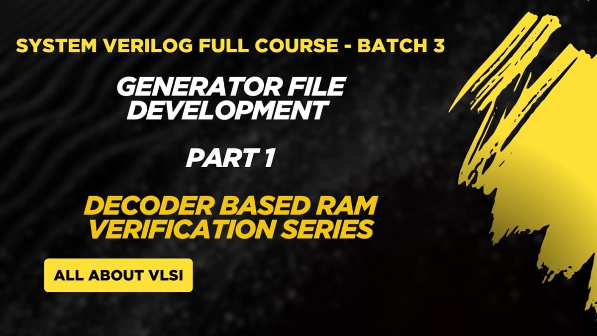
SystemVerilog Testbench | Generator File Development (Part 1) | SV Testbench for Decoder-Based RAM
The video walks through building a SystemVerilog testbench generator for a decoder‑based RAM, focusing on the code that creates and drives stimulus transactions. After reviewing the verification plan, interface, and transaction class, the presenter introduces the RAM_generator class, which encapsulates...