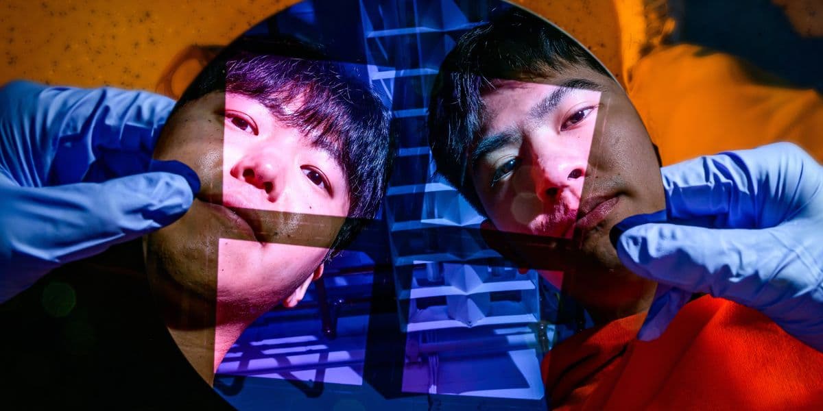
Junctionless Transistors Show a New Path to 3D Chips
Researchers at the University of Illinois Urbana‑Champaign have demonstrated a silicon‑based monolithic 3‑D chip built with junctionless transistors at temperatures below 200 °C using a roll‑transfer‑printing process. The technique stacks three layers of 10‑nm‑thin silicon membranes with sub‑10‑nm alignment, creating SRAM cells that are one‑third the footprint of comparable 2‑D designs and achieving current densities up to 650 mA/µm. By avoiding exotic materials and high‑temperature steps, the approach can integrate directly with existing foundry lines, potentially delivering denser, more energy‑efficient chips for AI and high‑performance computing. The work, published in Nature, outlines both performance gains and remaining challenges such as yield and thermal management.
The Next 15 Years of Moore’s Law, According to Imec
Imec’s new 15‑year roadmap predicts the commercial debut of complementary FET (CFET) technology around 2033, effectively stacking PMOS and NMOS devices to halve circuit area. The institute also foresees a shift to two‑dimensional semiconductor channels by 2041 to boost power...

Chip Fab-in-a-Box Could Democratize Semiconductors
InchFab, founded by MIT alumnus Mitchell Hsing, sells container‑size clean‑room systems priced between $5 million and $15 million. By scaling down to 4‑inch (100 mm) wafers, the startup shrinks traditional fab equipment, delivering a full suite of processes—including lithography, etch, and deposition—while accepting...

GPU Renters Are Playing a Silicon Lottery
Researchers from William & Mary, Jefferson Lab, and Silicon Data analyzed 3,500 GPUs across 11 cloud providers and found substantial performance variability even among identical models. The study, using the SiliconMark benchmark, showed up to a 34.5% difference in 16‑bit...

Terahertz Waves Spy on a Chip’s Internal Activity
Researchers at Adelaide University demonstrated a terahertz‑based system that can remotely monitor the electrical activity of transistors inside packaged chips. The setup uses a vector network analyzer, a terahertz frequency extender, and a homodyne quadrature receiver to detect minute changes...