
Key Takeaways
- •Cryogenic red LED illumination boosts GaAs 2DEG mobility
- •UV light (5 eV) further reduces disorder in hBN‑encapsulated graphene
- •Photo‑excited carriers fill trap states, improving screening of disorder
- •Enhanced transport reveals fragile fractional quantum Hall states
- •Empirical method lacks comprehensive theoretical model
Pulse Analysis
Disorder—variations in the crystal potential caused by vacancies, impurities, or interface roughness—sets the fundamental limit on electron mean free paths in low‑temperature 2D conductors. When lattice vibrations freeze out, scattering from these imperfections dominates, especially in semiconductor heterostructures where carrier screening is weak. Engineers therefore strive to create ultra‑clean environments, using techniques such as modulation doping and hBN encapsulation, to suppress the disorder potential and allow exotic many‑body states to emerge.
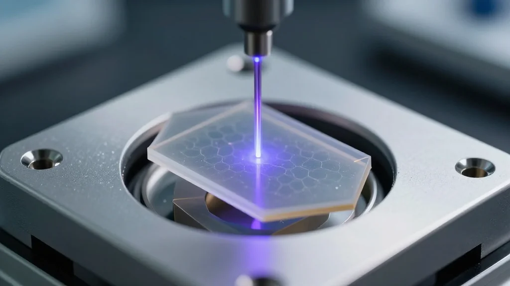
A practical, empirically proven shortcut to further reduce disorder is illumination at cryogenic temperatures. Decades of work on GaAs quantum wells show that a few minutes of red‑LED exposure near 10 K can dramatically increase mobility, as trapped charges are liberated and re‑distributed, smoothing the local potential landscape. Recent work extends this concept to graphene/hBN stacks, where deep‑UV photons (≈5 eV) achieve a comparable, if not greater, reduction in residual charge inhomogeneity despite being below hBN’s band gap. The result is sharper magnetotransport features and clearer signatures of fractional quantum Hall states, underscoring the technique’s versatility across material platforms.
The broader impact of illumination‑enhanced transport lies in its ability to unlock fragile quantum phenomena without costly redesigns of material growth or device architecture. Researchers can now probe higher‑order fractional states, explore interaction‑driven topological phases, and benchmark theoretical models with unprecedented precision. As the community seeks scalable quantum technologies, integrating controlled illumination steps into fabrication and measurement workflows could become a standard tool for achieving the ultra‑high mobility required for next‑generation 2D electronics.
Disorder and illumination
Comments
Want to join the conversation?