AI-Driven Design Tools Unlock New Capabilities in Flat Optical Devices
Why It Matters
By accelerating design cycles and embedding manufacturability, AI transforms metasurfaces into viable components for medical diagnostics, smart‑city sensors, and next‑generation communications, opening multi‑billion‑dollar market opportunities.
Key Takeaways
- •AI surrogate models predict nanostructure optics in milliseconds
- •Inverse design generates metasurface geometry from target optical specs
- •Integrated neural nets extract hyperspectral data for real‑time diagnostics
- •End‑to‑end co‑design yields cameras that self‑correct optical aberrations
- •Programmable metasurfaces enable adaptive camouflage and 6G smart antennas
Pulse Analysis
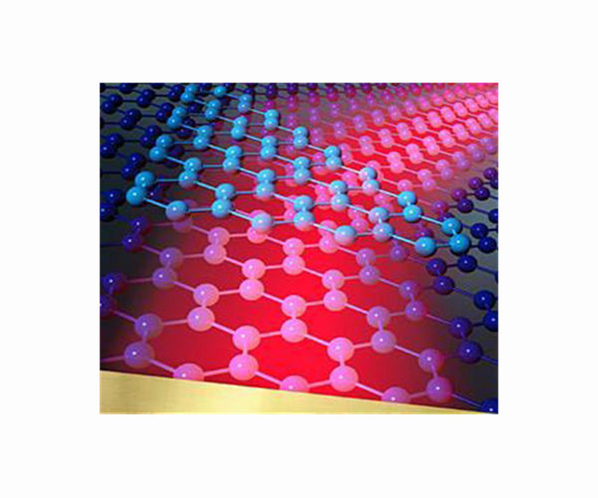
The rise of metasurfaces—nanostructured layers that manipulate light with sub‑wavelength precision—has long been hampered by a combinatorial design problem. Traditional electromagnetic solvers require days or weeks to evaluate a single geometry, making exhaustive exploration impractical. Recent advances in machine‑learning surrogate models compress that latency to milliseconds, allowing engineers to query optical responses instantly. Coupled with inverse design algorithms, designers now input a target focal length, bandwidth or phase profile and receive a manufacturable nanostructure layout, complete with tolerance constraints. This paradigm shift turns a trial‑and‑error process into a data‑driven workflow.
Accelerated design translates directly into new product possibilities. Integrated neural networks at the sensor level can decode the rich, multidimensional data generated by metasurfaces, enabling real‑time hyperspectral imaging for point‑of‑care blood analysis or atmospheric gas monitoring. In consumer electronics, co‑designed camera modules automatically correct aberrations, delivering sharper images without bulky lens assemblies. Programmable metasurfaces, steered by AI controllers, promise adaptive camouflage and reconfigurable antenna arrays that dynamically route 6G signals, reducing latency and spectrum congestion. These capabilities position metasurfaces as a cornerstone of the Internet of Things and smart‑city infrastructure.
Beyond functional advantages, metasurfaces offer a route to greener AI. Optical computing architectures can perform inference by routing photons through nanostrured patterns, consuming orders of magnitude less power than conventional silicon GPUs. Embedding such photonic processors alongside AI‑optimized metasurfaces could bring edge AI workloads within the energy envelope of battery‑powered devices. Industry analysts forecast a rapid expansion of the photonic‑AI market, with projected revenues exceeding $5 billion by 2030. Continued collaboration between photonics researchers and AI engineers will be essential to standardize design tools, scale manufacturing, and unlock the full commercial potential of flat optics.
AI-Driven Design Tools Unlock New Capabilities in Flat Optical Devices
Comments
Want to join the conversation?
Loading comments...