GaN: Boosting Optical Power Converter Efficiency
Why It Matters
The breakthrough makes high‑efficiency, wireless optical power transfer viable for aerospace, defense and rugged IoT deployments, expanding GaN’s role beyond lighting and power electronics. It also signals a path toward commercial‑scale production of compact, high‑temperature power converters.
Key Takeaways
- •Nichia's GaN converter reaches 60.2% efficiency at 45 W cm⁻².
- •Device maintains >60% efficiency from 20 to 96 W cm⁻² illumination.
- •Efficiency stays above 55% at 125 °C, showing temperature resilience.
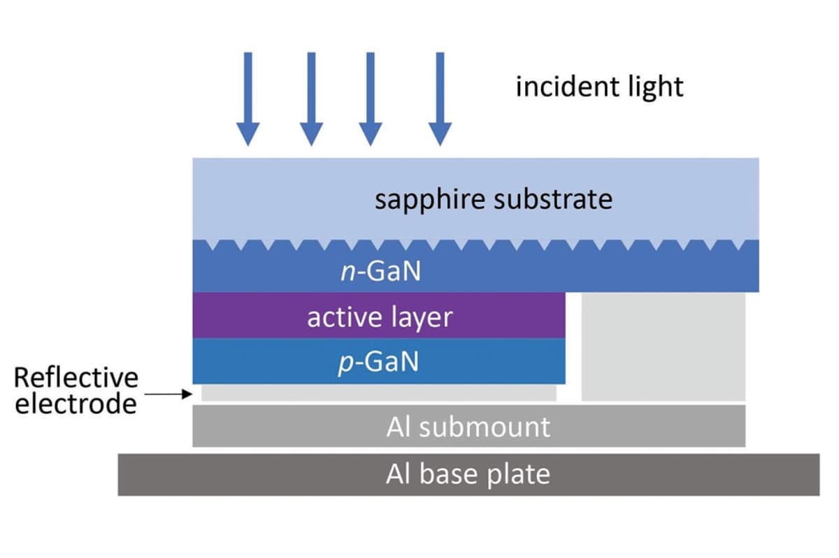
- •Design mirrors high‑power LEDs with 60 In₀.₁₂Ga₀.₈₈N/GaN quantum‑well pairs.
- •Reverse‑leakage current as low as 20 nA cm⁻² indicates high crystal quality.
Pulse Analysis
Optical power converters translate light into electricity, offering a wireless alternative when conventional wiring or batteries are impractical. Historically, the technology relied on gallium arsenide (GaAs) or indium‑gallium‑phosphide (InGaP) materials, which limited temperature tolerance and radiation resistance. Gallium‑nitride, already dominant in high‑brightness LEDs and power transistors, brings superior thermal conductivity and a wider bandgap, making it a natural candidate for robust converters. However, achieving high fill factors and low contact resistance in thick quantum‑well structures has been a persistent hurdle, keeping efficiencies below 45 percent.
Nichia’s latest device overcomes these obstacles by adapting its high‑power LED epitaxy process to an optical‑converter architecture. The chip, only 1.4 mm square, incorporates 60 alternating 2 nm In₀.₁₂Ga₀.₈₈N and 2.3 nm GaN layers, optimized for a 420 nm absorption edge. This configuration, combined with flip‑chip bonding to an aluminum‑nitride sub‑mount and a reflective rear electrode, enables multiple internal reflections that boost absorption without additional coatings. Under a modest –2 V bias, reverse‑leakage stays at 20 nA cm⁻², confirming excellent crystal quality, while external quantum efficiency peaks at 80 percent near 400 nm. The result is a stable 60 percent conversion efficiency across a broad intensity range and resilience up to 125 °C, positioning the technology for aerospace and other harsh‑environment applications.
The commercial implications are significant. High‑efficiency GaN converters could power remote sensors, satellite subsystems, or defense equipment without bulky batteries, reducing weight and extending mission lifespans. Their compatibility with existing GaN LED manufacturing lines promises economies of scale, potentially lowering costs for mass‑market wireless power solutions such as indoor IoT networks. As the industry pushes toward higher voltage, higher frequency power electronics, integrating optical converters with GaN transistors may enable fully solid‑state, optically isolated power architectures. Continued research on multi‑quantum‑well optimization and low‑resistance contacts will likely push efficiencies beyond the current 60 percent ceiling, accelerating adoption across multiple sectors.
GaN: Boosting optical power converter efficiency
Comments
Want to join the conversation?
Loading comments...