Laser Method Unlocks 3,000-Kelvin Thin-Film Synthesis for Quantum Materials
Why It Matters
TLE removes a long‑standing temperature barrier, enabling cost‑effective, high‑quality thin‑film production for quantum‑grade superconductors, accelerating the scaling of quantum hardware.
Key Takeaways
- •Laser evaporation deposits ultra‑refractory films at ~3,000 K temperatures
- •Technique uses focused 1‑kW fiber laser to melt pellet core
- •Resulting nickel films match or exceed quality of conventional methods
- •Enables scalable production of niobium and tantalum layers for quantum chips
Pulse Analysis
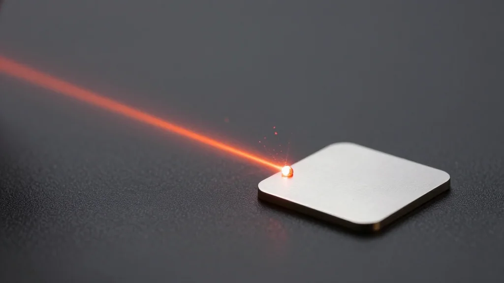
Thin‑film deposition underpins everything from semiconductor wafers to everyday packaging, yet materials with melting points above 2,500 K have remained out of reach for conventional vapor‑phase techniques. Traditional thermal evaporation requires heating an entire source to extreme temperatures, a process that quickly exceeds the limits of crucibles and containment vessels. The new laser‑based thermal evaporation (TLE) sidesteps this constraint by concentrating megawatt‑scale photon energy onto a microscopic spot of a solid pellet, creating a localized melt zone that vaporizes just enough material to form a uniform film. This approach leverages advances in high‑power fiber lasers originally developed for metal cutting, repurposing them for precision materials science.
In the proof‑of‑concept study, the Caltech team focused a 1‑kilowatt laser on a nickel target inside a vacuum chamber, achieving a melt temperature close to nickel’s 1,728 K. The resulting ultrathin film displayed electrical conductivity on par with, and in some measurements surpassing, films produced by sputtering or electron‑beam evaporation. Crucially, the process maintains the bulk of the source material solid, reducing waste and extending the usable lifetime of expensive refractory alloys. The localized heating also minimizes thermal stress on the substrate, preserving surface integrity—a key factor for quantum‑grade superconducting circuits.
The implications for the quantum computing ecosystem are significant. Superconducting qubits rely on niobium, tantalum, and related alloys, all of which melt above 3,000 K and have been difficult to coat uniformly. TLE offers a scalable pathway to deposit these ultra‑refractory layers with high purity and low defect density, potentially lowering fabrication costs and improving qubit coherence times. As the industry pushes toward larger quantum processors, the ability to produce reliable, high‑performance thin films could become a competitive differentiator, spurring broader adoption of laser‑driven deposition across semiconductor and photonics manufacturing.
Laser method unlocks 3,000-Kelvin thin-film synthesis for quantum materials
Comments
Want to join the conversation?
Loading comments...