Metasurface Plus Photoelectric Quantum Effect Yields Sensitive THz Detector
Companies Mentioned
Why It Matters
The breakthrough narrows the longstanding ‘THz gap,’ enabling more sensitive, compact terahertz sensors that can lower system cost and expand applications in imaging, communications, and spectroscopy.
Key Takeaways
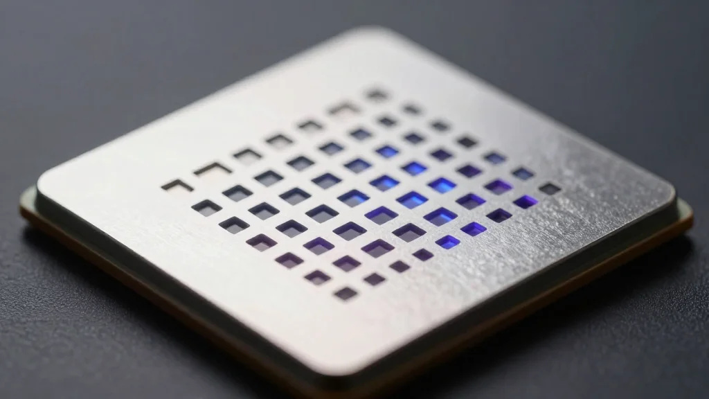
- •Metasurface concentrates THz waves into sub‑wavelength detector gaps
- •In‑plane photoelectric effect yields current without photon energy threshold
- •Responsivity reaches 2.7 A/W, 20× improvement over earlier PETS devices
- •Fabrication aligns with existing transistor processes, easing commercial scaling
Pulse Analysis
The terahertz portion of the electromagnetic spectrum—roughly 0.1 to 10 THz—has long been called the “THz gap” because conventional electronic components struggle with the high frequencies while optical technologies are mismatched to the long wavelengths. This gap hampers the development of compact imaging, high‑speed wireless links, and spectroscopic sensors that could transform security screening, pharmaceutical analysis, and next‑generation communications. Existing detectors often rely on bulky antennas, cryogenic cooling, or require photons to exceed a strict energy threshold, limiting sensitivity and driving up system cost.
The Cambridge‑Swansea team sidestepped these constraints by marrying a metasurface with the recently discovered in‑plane photoelectric effect (IPPE). The brick‑work metasurface acts as a sub‑wavelength antenna array, funneling incident THz energy into narrow capacitive gaps where photoelectric tunable‑step (PETS) elements sit. Because the IPPE does not demand a minimum photon energy, electrons in the two‑dimensional electron gas can be excited directly, producing a measurable current. In a proof‑of‑concept cooled to 10 K, the detector delivered 2.7 A/W responsivity and 2.1 % external quantum efficiency at 1.9 THz—about twenty times the performance of earlier PETS prototypes.
Beyond the impressive lab numbers, the device’s fabrication mirrors standard high‑mobility field‑effect transistor processes, suggesting a clear path to wafer‑scale production and on‑chip integration with existing silicon‑based circuitry. Eliminating external lenses or waveguides reduces assembly complexity and cost, making THz imaging modules more viable for commercial markets. If future work raises the operating temperature to levels achievable with compact cryocoolers, the technology could underpin portable spectrometers, non‑destructive testing tools, and ultra‑high‑bandwidth wireless links. The convergence of metasurface engineering and quantum‑enhanced detection therefore marks a pivotal step toward closing the THz gap.
Metasurface plus photoelectric quantum effect yields sensitive THz detector
Comments
Want to join the conversation?
Loading comments...