Monash Researchers Unveil Room‑Temperature Photonic Valleytronic Chip
Why It Matters
The chip demonstrates that photonic computing can move beyond isolated components to fully integrated systems, a prerequisite for practical adoption. By operating at room temperature, it sidesteps the costly cooling infrastructure that hampers many quantum‑based approaches, making it more attractive for data‑center and AI hardware where energy efficiency is paramount. Moreover, the use of valleytronic encoding expands the toolbox for encoding information, potentially enabling denser data representation and new security paradigms. If the technology scales, it could reshape the semiconductor roadmap, prompting a shift from electron‑centric designs to hybrid platforms that leverage light for high‑speed, low‑power processing. This would have ripple effects across cloud services, edge devices, and emerging quantum‑information applications, accelerating the overall pace of innovation in the science and technology sectors.
Key Takeaways
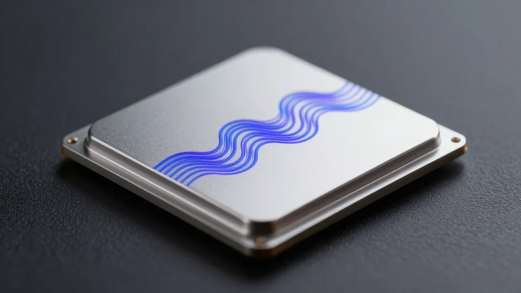
- •Monash University scientists built a chip that generates, routes and reads light signals on a single platform.
- •The device uses the valley degree of freedom in ultra‑thin materials to encode information.
- •It operates at room temperature, eliminating the need for cryogenic cooling.
- •Demonstrated simultaneous processing of two images, showing parallel data handling.
- •Researchers aim to partner with manufacturers for pilot production and scaling.
Pulse Analysis
The Monash photonic valleytronic chip arrives at a moment when the industry is grappling with the limits of Moore's Law and the energy ceiling of conventional silicon transistors. Photonic approaches have long promised higher bandwidth and lower heat, but integration challenges have kept them in the research domain. By consolidating generation, routing, and detection, the Monash team effectively collapses the photonic stack into a single silicon‑compatible footprint, a move that could lower the entry barrier for chipmakers.
Historically, valleytronics has been a niche within quantum materials research, largely confined to low‑temperature experiments. The room‑temperature operation demonstrated here signals a maturation that aligns with the commercial timelines of silicon photonics, which has already seen adoption in data‑center interconnects. The key differentiator is the ability to encode information in quantum valleys, offering a new dimension of data density and potentially novel encryption methods. If industry partners can translate the lab‑scale stacking technique into high‑volume manufacturing, we may see a new class of hybrid chips that blend electronic logic with photonic data paths, delivering the speed gains needed for next‑generation AI workloads.
Looking ahead, the biggest hurdle will be economic: the cost of ultra‑thin material synthesis and metasurface fabrication must compete with established silicon photonic processes. However, the promise of reduced power consumption—critical for the exploding energy demands of AI training—could justify the investment. In the next 12‑18 months, we should watch for pilot fab runs, performance benchmarks against silicon photonic links, and any strategic alliances between academic groups and semiconductor giants. Successful scaling would not only validate valleytronics as a viable computing paradigm but also accelerate the broader transition toward light‑based information processing across the tech ecosystem.
Monash Researchers Unveil Room‑Temperature Photonic Valleytronic Chip
Comments
Want to join the conversation?
Loading comments...