NIST Researchers Develop Photonic Chip Packaging
Why It Matters
The breakthrough makes high‑speed, low‑power photonic technology usable in quantum computing, space, and nuclear environments, opening new markets for photonic sensors and communications. It also resolves a long‑standing reliability barrier, potentially accelerating adoption of photonics in extreme‑condition industries.
Key Takeaways
- •NIST applies hydroxide catalysis bonding to photonic chip packaging
- •Bond forms inorganic glass-like link, resisting radiation, vacuum, temperature extremes
- •Packaged chips survived cryogenic temps, rapid thermal swings, ionizing radiation
- •Enables photonic circuits for quantum computers, space missions, nuclear reactors
- •Process currently takes days; engineering improvements could speed up manufacturing
Pulse Analysis
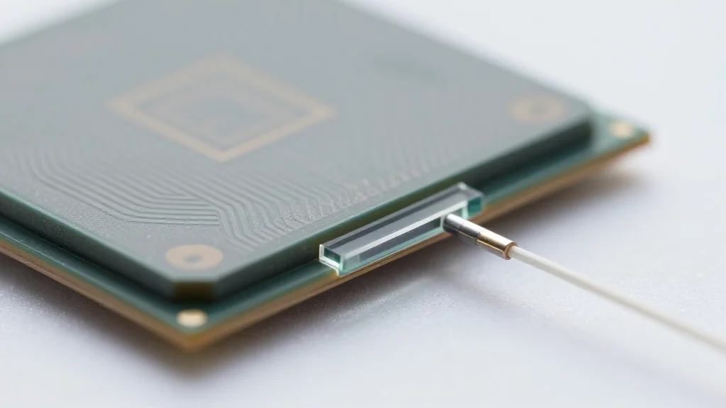
Photonic integrated circuits are reshaping data transmission by using light instead of electricity, delivering higher bandwidth with lower power consumption. However, their commercial expansion has been hampered by fragile packaging that cannot survive the harsh environments required by quantum processors, space telescopes, or nuclear facilities. Traditional polymer adhesives crack or outgas under extreme temperature swings, radiation, and vacuum, breaking the precise alignment needed for efficient optical coupling. NIST’s adoption of hydroxide catalysis bonding (HCB) replaces these organic glues with a glass‑like inorganic bond, preserving sub‑micron alignment while withstanding conditions that would destroy conventional packages.
The HCB technique, borrowed from NASA’s ultra‑stable optical assemblies, employs a minute sodium hydroxide solution to fuse the fiber and chip surfaces at the molecular level. In rigorous lab trials, the bonded assemblies endured cryogenic cooling near absolute zero, rapid thermal cycling between hot and cold, intense ionizing radiation, and high‑vacuum environments without loss of optical performance. These results prove that photonic chips can now operate reliably where they previously could not, unlocking new possibilities for quantum‑hardware interconnects, deep‑space communication links, and sensors embedded in reactors or particle accelerators. The method also maintains the high‑speed, low‑loss characteristics that make photonics attractive for next‑generation networks.
From a market perspective, this packaging breakthrough could catalyze a wave of photonic products targeting sectors that demand extreme resilience. Quantum computing platforms, which often run at millikelvin temperatures, could integrate photonic interconnects for faster qubit control and readout. Space agencies may adopt photonic links for satellite constellations, reducing weight and power budgets. Meanwhile, industrial and energy firms could deploy photonic sensors for real‑time monitoring in high‑temperature or high‑radiation settings. Although the current bonding process spans several days, NIST anticipates engineering refinements will shorten cycle times, making the technology scalable for volume manufacturing and accelerating its commercial rollout.
NIST Researchers Develop Photonic Chip Packaging
Comments
Want to join the conversation?
Loading comments...