Perovskite Diode Sets Records as Both a Solar Cell and an LED
Why It Matters
By solving the long‑standing trade‑off between light emission and absorption, the technology enables products that can harvest energy and emit light with a single, low‑cost component, reshaping the economics of next‑generation displays and lighting.
Key Takeaways
- •Perovskite diode reaches 26.7% solar efficiency and 31% LED EQE
- •Electrostatic alumina islands enable light routing without blocking charge
- •Surface passivation drops recombination velocity to 1.4 cm/s
- •Device retains 95% efficiency after 1,200 hours, surpassing flat control
- •Dual‑function architecture opens path for self‑powered displays
Pulse Analysis
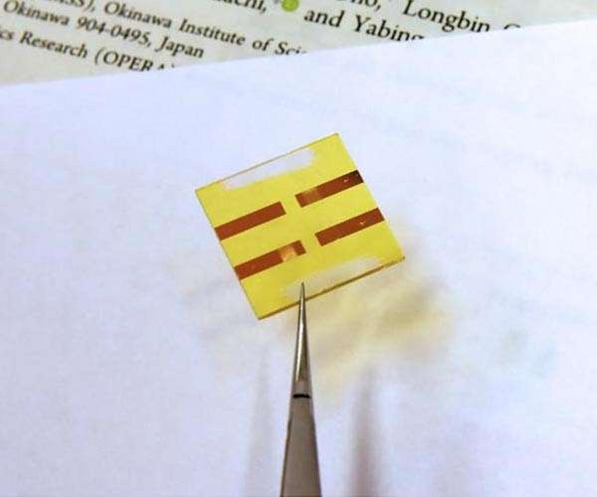
Perovskite semiconductors have surged in the past decade as a cheap, tunable alternative to silicon and III‑V compounds for both photovoltaics and solid‑state lighting. Historically, the optimal layer thickness for a solar cell—tens of nanometers thick enough to absorb sunlight—conflicted with the ultra‑thin, scattering‑friendly films needed for efficient LEDs. This inherent design tension limited the commercial appeal of devices that could do both, relegating the two markets to separate material stacks.
The new study resolves that conflict by embedding porous alumina nanoplates—assembled via opposite electrostatic charges—into a single 800 nm perovskite layer. These e‑Al₂O₃ islands act as low‑refractive‑index scaffolds that guide photons outward while allowing the perovskite to maintain electrical continuity. Simultaneously, the surface‑treating molecules that charge the particles also passivate defect sites, slashing surface recombination velocity from 20.2 cm/s to 1.4 cm/s. With defects minimized, photon recycling becomes significant, further boosting external quantum efficiency beyond geometric expectations.
The implications extend far beyond the lab. A dual‑function diode that rivals the performance of expensive single‑crystal gallium arsenide could power self‑lit displays that harvest ambient light, extend battery life in wearables, or create lighting fixtures that feed excess energy back into the grid. Because the perovskite process remains low‑temperature and solution‑based, scaling to large‑area manufacturing is far more feasible than for traditional III‑V wafers. As the industry seeks sustainable, cost‑effective optoelectronic solutions, this co‑optimized architecture positions perovskites as a credible contender for the next wave of integrated energy‑light devices.
Perovskite Diode Sets Records as Both a Solar Cell and an LED
Comments
Want to join the conversation?
Loading comments...