Photoexcitation Flips 2D Moiré Devices From Metals to Insulators in Ultrafast Test
Why It Matters
Reversing the usual insulator‑to‑metal photo‑switch expands the toolbox for quantum device engineering, allowing sub‑nanosecond control of electronic phases essential for scaling optoelectronic quantum technologies.
Key Takeaways
- •Photoexcitation flips WS₂/WSe₂ moiré devices from metal to insulator
- •Hot holes from graphite gates drive the ultrafast transition
- •Transition occurs within picoseconds, enabling sub‑nanosecond control
- •Opens pathway for ultrafast quantum memory and processors
Pulse Analysis
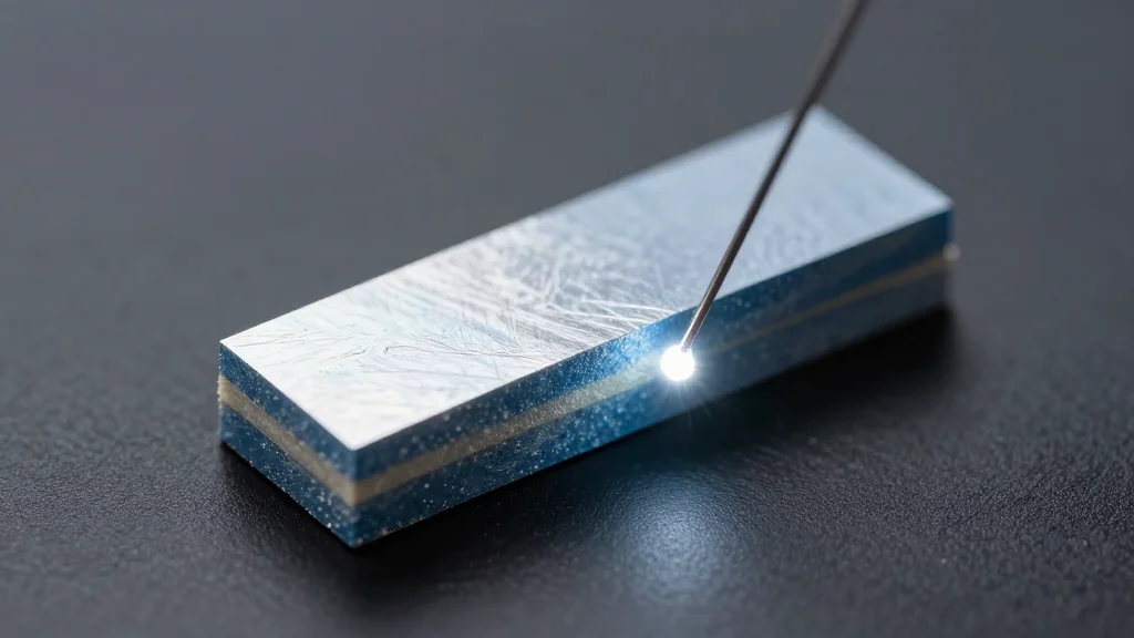
The discovery of light‑driven phase transitions has become a cornerstone of quantum‑materials research, offering a route to switch electronic states without physical contacts. Two‑dimensional moiré heterostructures—formed by stacking atomically thin layers with a slight twist—exhibit strongly correlated phases that can be tuned by carrier density, pressure or electric fields. Until now, most optical studies reported insulator‑to‑metal transitions, where photons inject carriers that melt a correlated gap. The new work flips this paradigm by demonstrating a metal‑to‑insulator switch, a capability that broadens the functional palette of moiré platforms.
In the Columbia‑UC Riverside study, researchers assembled WS₂/WSe₂ bilayers with graphite gate electrodes and probed them using femtosecond pump‑probe spectroscopy. An initial high‑intensity pump pulse doped the stack into a metallic state; a subsequent pulse generated hot holes in the graphite, which were injected into the moiré lattice within a few picoseconds. This ultrafast hole transfer disrupted the correlated electron network, reopening the Mott‑like gap and producing a clear insulating signature in the reflectivity spectrum. The ability to toggle carrier density on a picosecond clock marks a technical leap for quantum‑phase control.
The metal‑to‑insulator switch opens several pathways for next‑generation devices. Ultrafast optical control of a correlated gap could serve as the basis for quantum memory elements that write and erase states in sub‑nanosecond intervals, dramatically reducing latency compared with conventional charge‑based storage. Moreover, integrating such moiré switches into photonic circuits may enable reconfigurable quantum processors where logical operations are encoded in transient electronic phases. Future work will likely explore other twisted‑layer combinations, scaling to wafer‑level fabrication, and coupling to superconducting qubits, positioning photo‑driven moiré engineering at the forefront of quantum technology roadmaps.
Photoexcitation flips 2D moiré devices from metals to insulators in ultrafast test
Comments
Want to join the conversation?
Loading comments...