Quantum Metasurface Boosts Terahertz Detection Sensitivity by Exploiting In-Plane Photoelectric Effect
Why It Matters
By delivering high sensitivity without cryogenic cooling or bulky optics, the quantum metasurface detector could accelerate adoption of terahertz technology in communications, security screening, and biomedical imaging.
Key Takeaways
- •Metasurface design yields 20× sensitivity boost over prior PETS detectors
- •Responsivity reaches 2.7 A W⁻¹ with 2.1 % external quantum efficiency at 1.9 THz
- •Detector operates at zero bias, eliminating dark‑current noise
- •Fabrication compatible with standard semiconductor processes, enabling on‑chip integration
- •Scalable architecture can target frequencies from microwave to mid‑infrared
Pulse Analysis
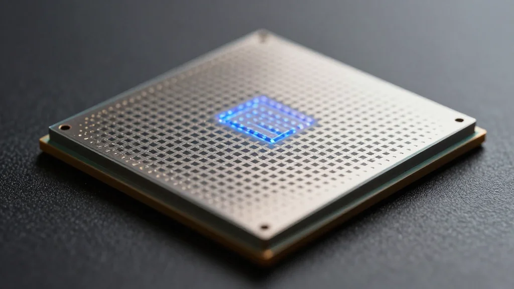
Terahertz (THz) radiation sits between microwave and infrared frequencies, offering unique capabilities for high‑speed wireless links, non‑destructive testing, and medical diagnostics. Yet the market has been hampered by detectors that are either sluggish, require cryogenic cooling, or depend on cumbersome external optics. The new quantum metasurface detector sidesteps these constraints by embedding the light‑capture function directly into a patterned surface, leveraging the in‑plane photoelectric effect to convert THz photons into electrical current without a voltage bias. This integration reduces system complexity and opens the door to compact, low‑noise THz modules.
The core innovation lies in marrying a two‑dimensional electron gas with a “brickwork” metasurface that funnels electromagnetic energy into narrow capacitive gaps. Each gap hosts a PETS element, and the collective output of hundreds of these micro‑detectors yields a responsivity of 2.7 A W⁻¹—far surpassing earlier PETS prototypes. With an external quantum efficiency of 2.1 % at 1.9 THz, the device demonstrates a 20‑fold sensitivity improvement, all while operating at 10 K, a temperature reachable with compact cryocoolers rather than liquid helium. The zero‑bias operation eliminates dark currents, further enhancing signal‑to‑noise ratios.
Beyond performance metrics, the detector’s fabrication mirrors conventional field‑effect transistor processes, allowing seamless integration onto silicon chips and scaling across the electromagnetic spectrum. Manufacturers can envision THz imaging arrays, on‑chip spectrometers, or secure communication front‑ends that fit within existing semiconductor supply chains. As the THz gap narrows, this quantum metasurface approach positions itself as a catalyst for commercializing applications ranging from high‑capacity 6G networks to rapid quality‑control inspections in factories, potentially reshaping multiple high‑tech sectors.
Quantum metasurface boosts terahertz detection sensitivity by exploiting in-plane photoelectric effect
Comments
Want to join the conversation?
Loading comments...