Recent Advances in Topological Materials for Photodetection
Why It Matters
These advances could replace conventional semiconductor detectors, delivering faster, more sensitive imaging for communications, security, and scientific instrumentation while opening new markets for integrated photonic systems.
Key Takeaways
- •Topological photodetectors cover visible to terahertz spectra.
- •Surface states boost carrier mobility and ultrafast response.
- •Reported responsivity exceeds 10 A/W, response <1 ps.
- •Synthesis complexity and dark‑current remain major hurdles.
Pulse Analysis
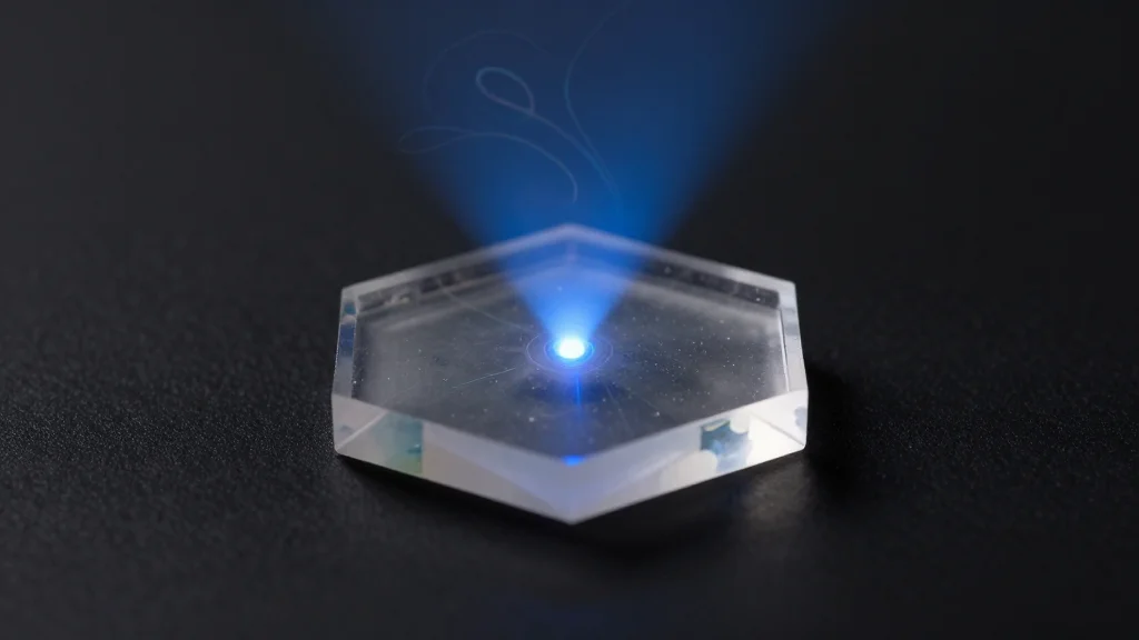
Topological materials have reshaped the photodetector landscape by leveraging nontrivial band structures and protected surface states. Unlike traditional semiconductors, these materials enable direct coupling between light and high‑mobility carriers, producing broadband photoresponse that spans from the visible range through infrared to terahertz frequencies. Researchers have demonstrated that topological insulators and Dirac semimetals can achieve responsivities above 10 A/W and sub‑picosecond rise times, positioning them as candidates for next‑generation high‑speed imaging and communication systems.
The performance edge stems from two intertwined mechanisms. First, topological surface states provide linear dispersion and reduced scattering, granting carriers exceptional mobility that translates into ultrafast electrical signals. Second, bulk‑state contributions can be engineered to extend spectral absorption, allowing devices to operate across multiple wavelength bands without complex multilayer stacks. Device architectures ranging from planar photoconductors to waveguide‑integrated detectors have been reported, each exploiting the unique light‑matter interaction to surpass conventional silicon or III‑V photodiodes in speed and sensitivity.
Despite these gains, practical deployment faces material‑level obstacles. High‑quality crystal growth remains costly and yields limited wafer‑scale uniformity, while intrinsic dark current from bulk defects hampers signal‑to‑noise ratios. Addressing these issues will require advances in epitaxial techniques, passivation strategies, and scalable fabrication processes. As these hurdles recede, topological photodetectors are poised to drive growth in sectors such as autonomous vehicle LiDAR, secure terahertz communications, and biomedical imaging, where rapid, low‑noise detection is paramount.
Recent Advances in Topological Materials for Photodetection
Comments
Want to join the conversation?
Loading comments...