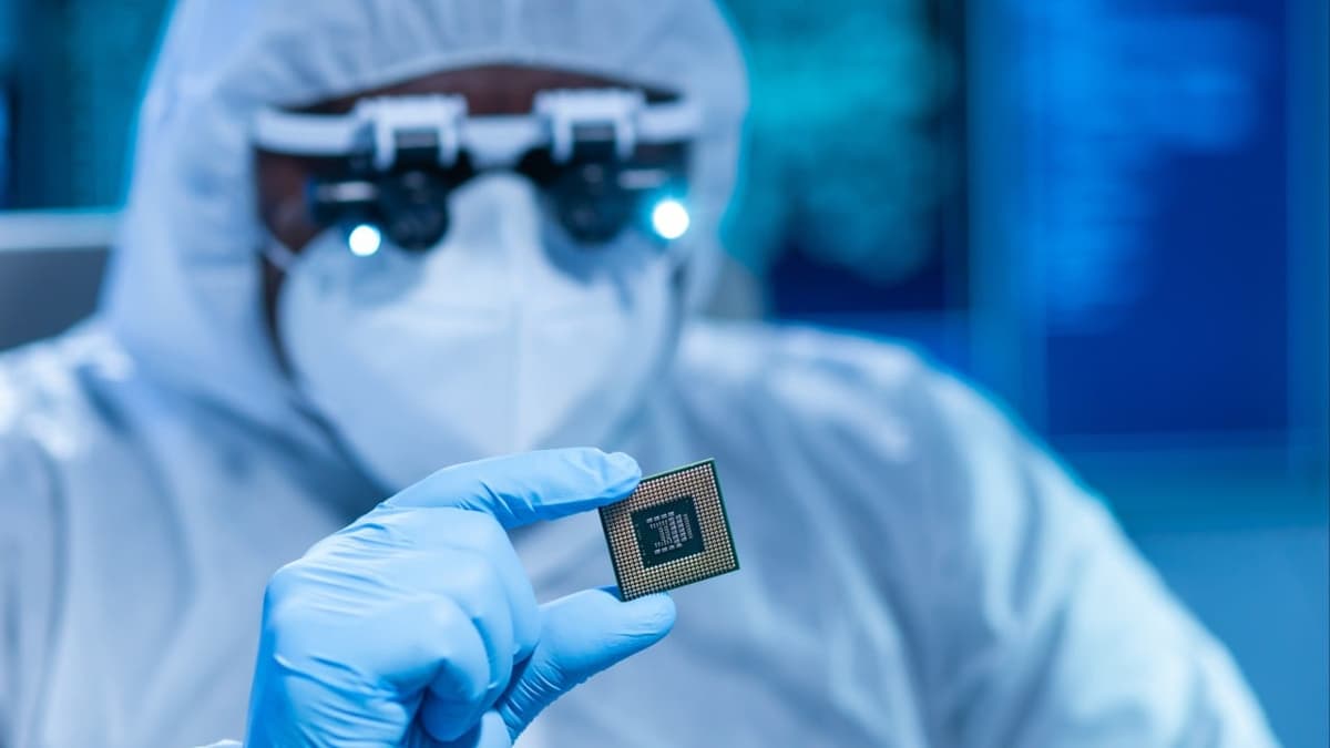
Semiconductor Leap: China Looks to Next-Gen ‘2D Chip’ with 1,000-Fold Growth Speed
Companies Mentioned
Why It Matters
The ultra‑fast, wafer‑scale 2D growth could dramatically lower costs and speed up adoption of next‑generation chips, strengthening China’s semiconductor self‑sufficiency and reshaping the global supply chain.
Key Takeaways
- •Wafer-scale 2D chips grown 1,000× faster than prior methods
- •Technique could cut production costs and accelerate mass‑manufacturing
- •Enables high‑performance LEDs, photodetectors, and lasers for optoelectronics
- •Positions China closer to semiconductor self‑sufficiency amid US restrictions
- •Industry analysts expect post‑Moore devices within next five years
Pulse Analysis
The race to commercialize two‑dimensional semiconductors has long been hampered by slow, small‑area growth techniques that limited their economic viability. The new wafer‑scale process, reportedly based on an advanced chemical vapor deposition platform, slashes crystal formation time by three orders of magnitude while maintaining uniformity across full 200‑mm wafers. This leap addresses the critical bottleneck of scalability, allowing manufacturers to integrate 2D layers directly into existing fab lines and to explore heterostructures that combine the best of graphene, transition‑metal dichalcogenides, and other emerging materials.
China’s semiconductor strategy has increasingly focused on reducing reliance on foreign equipment and intellectual property. By achieving rapid, large‑area 2D growth, the country can potentially produce high‑performance optoelectronic components—key for data‑center interconnects, LiDAR, and next‑generation displays—without importing costly foreign fabs. The cost advantage of a 1,000‑fold speed increase could translate into lower price points for LEDs and photodetectors, eroding the market share of established players in the United States, Taiwan, and South Korea. Moreover, the technology aligns with Beijing’s "Made in China 2025" goals, offering a home‑grown pathway to advanced chip architectures that bypass traditional silicon scaling limits.
Looking ahead, the challenge will shift from growth speed to integration and yield. Defect density, interface engineering, and thermal management remain critical hurdles before 2D chips can meet the reliability standards of automotive or AI accelerator markets. Nevertheless, the breakthrough opens a realistic timeline for post‑Moore devices, with pilot production lines expected within the next two to three years. If industry partners can standardize design‑for‑2D processes, the technology could underpin a new class of ultra‑thin, low‑power processors that redefine performance benchmarks across consumer electronics, telecommunications, and autonomous systems.
Semiconductor leap: China looks to next-gen ‘2D chip’ with 1,000-fold growth speed
Comments
Want to join the conversation?
Loading comments...