“Solving the Ultra-Thin Challenge: Contact Resistance Reduced 50×, On-State Current Boosted 17×”
Why It Matters
By overcoming the contact‑resistance bottleneck, the technique enables faster, lower‑power ultra‑thin devices that can be manufactured at scale, accelerating the rollout of next‑generation 3D chips for data‑intensive workloads.
Key Takeaways
- •Contact resistance fell from 97.5 kΩ·µm to 1.7 kΩ·µm.
- •On‑state current increased over 17× at –196 °C.
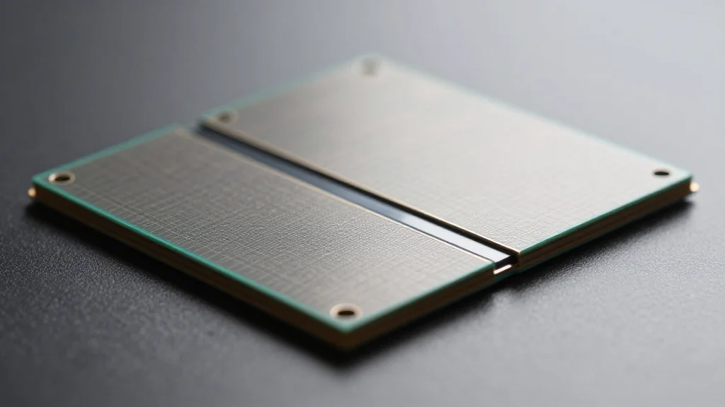
- •Raised source/drain (RSD) selectively thickens tellurium at contacts.
- •Sputtering enables low‑temperature, large‑area manufacturing compatibility.
- •Approach supports 3D IC stacking below 400 °C for AI workloads.
Pulse Analysis
The race to shrink semiconductor channels below five nanometers has hit a fundamental wall: as the channel thins, the metal‑semiconductor interface becomes increasingly resistive, throttling speed and raising power consumption. Tellurium, with its high carrier mobility and room‑temperature stability, emerged as a promising candidate, yet its narrow band gap demanded ultra‑thin channels to curb leakage. Traditional silicon tricks, however, did not translate directly, leaving engineers searching for a method to preserve the channel’s electrostatic control while easing electron injection.
POSTECH’s solution revives the classic raised source/drain (RSD) concept, but applies it to a two‑dimensional material. By locally thickening the tellurium at the source and drain, the team creates a low‑resistance conduit that bypasses the Schottky barrier expansion typical of ultra‑thin devices. Laboratory measurements show contact resistance collapsing from 97.5 kΩ·µm to just 1.7 kΩ·µm, and a 17‑fold surge in on‑state current when cooled to –196 °C. Crucially, the process relies on sputtering—a scalable, low‑temperature deposition technique—allowing seamless integration into existing fab lines without costly retooling.
The broader impact reaches beyond a single material breakthrough. Reliable, low‑resistance ultra‑thin transistors are a prerequisite for dense 3D integrated circuits, where logic and memory are stacked to cut latency and energy use. The RSD approach meets the sub‑400 °C thermal budget of 3D stacking, positioning tellurium devices as viable building blocks for AI accelerators and high‑performance computing platforms. As the industry pivots toward heterogeneous integration, this band‑engineering strategy could be adapted to other emerging 2D semiconductors, catalyzing a new wave of nano‑electronic innovation.
“Solving the ultra-thin challenge: Contact resistance reduced 50×, on-state current boosted 17×”
Comments
Want to join the conversation?
Loading comments...