Twisted Stacking Lets 2D Conductor Keep Single-Layer Performance in Bulk Form
Why It Matters
By enabling bulk 2D conductors to retain single‑layer performance, the discovery removes a key barrier to commercializing next‑generation semiconductors and quantum‑material technologies, accelerating their entry into real‑world applications.
Key Takeaways
- •Twisted stacking prevents interlayer electron scattering in multilayer MOFs.
- •Ni₃(HITrip)₂ retains Dirac Kagome band structure in bulk form.
- •Measured conductivity reaches 0.58 S · cm⁻¹ without doping.
- •Enables scalable manufacturing of high‑performance 2D‑based electronics.
- •Opens pathway for bulk quantum and topological material applications.
Pulse Analysis
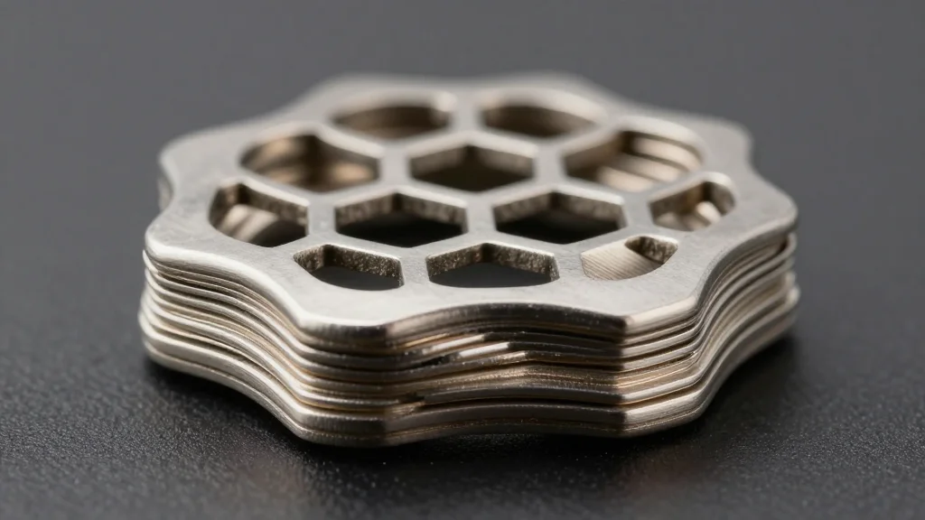
Two‑dimensional materials have long promised ultra‑fast electron transport, but their promise stalls when layers are stacked, as interlayer coupling creates scattering centers that degrade conductivity. The concept of twisted stacking—introducing a deliberate angular misalignment between successive sheets—mirrors the success of twisted bilayer graphene, where a “magic angle” unlocks novel electronic phases. By applying this principle to a conductive metal‑organic framework, the KAIST‑Oregon team sidestepped the conventional trade‑off between thickness and performance, preserving the pristine electronic landscape of a single layer in a macroscopic crystal.
The resulting compound, Ni₃(HITrip)₂, incorporates a triptycene‑based ligand that enforces a staggered geometry, effectively decoupling adjacent layers. Spectroscopic and computational analyses confirm that the material retains the Dirac‑type Kagome band structure, a hallmark of high‑mobility carriers. Remarkably, the bulk crystal exhibits an intrinsic conductivity of 0.58 S · cm⁻¹ without extrinsic doping, rivaling many doped 2D conductors while simplifying processing. This performance stems from cooperative interactions between the nickel nodes and the conjugated organic scaffold, which together create a low‑energy pathway for electrons across the twisted lattice.
From a market perspective, the ability to produce bulk‑scale 2D conductors with single‑layer quality could reshape semiconductor manufacturing, flexible electronics, and quantum‑information platforms. Engineers can now envision wafer‑level integration of high‑mobility layers without the costly precision stacking required for heterostructures. Moreover, the preserved topological features open avenues for robust quantum devices that leverage protected edge states. As the industry seeks materials that combine scalability, high conductivity, and exotic quantum properties, twisted‑stacked MOFs like Ni₃(HITrip)₂ are poised to become a cornerstone of next‑generation electronic architectures.
Twisted stacking lets 2D conductor keep single-layer performance in bulk form
Comments
Want to join the conversation?
Loading comments...