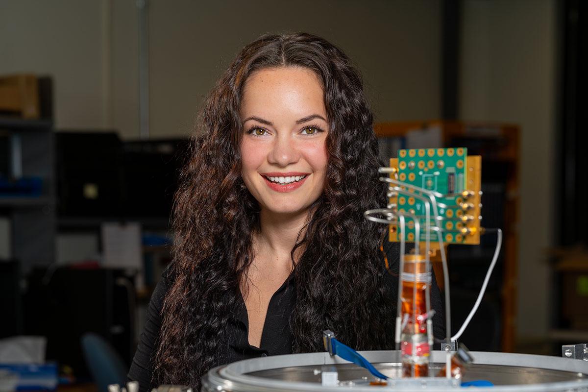
Using AI, Fermilab Researcher Probes How Transistors Behave in Extreme Cold
Why It Matters
Accelerating cryogenic transistor modeling removes a major bottleneck for quantum‑computing hardware and space‑qualified electronics, giving U.S. innovators a speed advantage in emerging high‑value markets.
Key Takeaways
- •AI model predicts cryogenic transistor parameters in ~120 milliseconds.
- •Traditional modeling can take weeks to months, often two years.
- •Faster models enable efficient design of quantum and space electronics.
- •Prototype built by Seidel reduces data generation to two weeks.
- •Genesis Mission funds AI-driven extreme‑environment chip research.
Pulse Analysis
Cryogenic electronics have moved from niche research to a cornerstone of next‑generation technologies. Quantum processors, superconducting photon detectors, and satellite‑grade sensors all require transistors that function reliably at temperatures just a few kelvins above absolute zero. At those extremes, carrier mobility, threshold voltage, and leakage currents shift dramatically, making room‑temperature models unreliable. Historically, engineers have spent months—sometimes years—tuning physics‑based models to match sparse measurement data, a process that slows product cycles and inflates development costs.
Seidel’s approach leverages machine‑learning algorithms to infer the underlying physics directly from laboratory measurements. By generating a curated training set over two weeks, the model learns the complex, non‑linear relationships governing cryogenic behavior. Once trained, it predicts a complete set of physics parameters in about 120 ms, delivering accuracy comparable to conventional methods. This dramatic reduction in turnaround time not only frees engineers from repetitive fitting tasks but also enables rapid exploration of new transistor architectures tailored for ultra‑low‑temperature operation.
The broader impact resonates across the DOE’s Genesis Mission, which seeks to embed AI across national‑lab research to accelerate high‑impact innovation. Faster, AI‑derived cryogenic models can shorten the path from silicon design to quantum‑ready hardware, lowering barriers for startups and established chipmakers alike. As the demand for quantum‑grade and space‑qualified electronics surges, the ability to iterate designs in days rather than years could cement U.S. leadership in these strategic sectors, while also reducing the energy and material waste associated with prolonged prototyping cycles.
Using AI, Fermilab researcher probes how transistors behave in extreme cold
Comments
Want to join the conversation?
Loading comments...