Van Der Waals Forces Can Play Unexpected Role in Thin Film Properties
Why It Matters
By providing a non‑chemical method to control key ferroelectric parameters, the work opens a pathway for scaling ultra‑thin, energy‑efficient memory and sensor technologies. It signals a shift toward vdW‑engineered heterostructures in next‑generation semiconductor manufacturing.
Key Takeaways
- •Van der Waals bonding lets SnSe films adopt varied orientations.
- •Strong vdW force on MoS₂ yields larger, defect‑reduced SnSe layers.
- •Thickness, strain, and domain architecture are jointly tuned by vdW strength.
- •Approach offers a non‑chemical pathway for ferroelectric device mini‑scaling.
Pulse Analysis
Ferroelectric thin films are a cornerstone of emerging low‑power memory, sensors, and actuation technologies because their spontaneous polarization can be switched with minimal energy. Yet achieving high‑quality epitaxial layers at nanometer scales remains difficult; conventional epitaxy relies on strong chemical bonds that force the overlayer to adopt the substrate’s lattice, often introducing strain or defects when the two crystals are mismatched. Researchers have therefore been exploring alternative bonding mechanisms that can relax these constraints while preserving crystalline order.
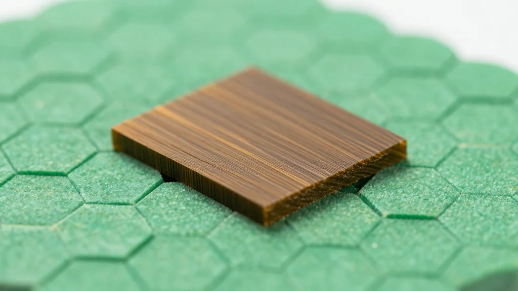
In a June 2026 paper in ACS Nano, a team led by NC State’s Yin Liu demonstrated that van der Waals (vdW) forces can serve as that alternative. By depositing tin selenide (SnSe) on a monolayer of molybdenum disulfide (MoS₂), they exploited the near‑perfect lattice match that yields a relatively strong vdW interaction. The study showed that the vdW bond directly influences three key parameters—film thickness, atomic‑scale strain, and domain architecture—allowing the researchers to grow larger, smoother SnSe layers with markedly fewer defects than on weaker‑bonded substrates such as graphene.
The ability to tune ferroelectric properties through a non‑chemical interface opens a practical design knob for next‑generation electronics. Device engineers can now consider vdW‑engineered substrates to fine‑tune polarization behavior without sacrificing film integrity, a prospect that could accelerate the rollout of ultra‑thin non‑volatile memories and low‑energy logic gates. As the semiconductor industry pushes toward heterogeneous integration of 2D materials, the NC State findings provide a roadmap for leveraging vdW forces across a broader palette of ferroelectric compounds, prompting further exploration of substrate‑film combos that balance lattice alignment with controllable interlayer attraction.
Van der Waals forces can play unexpected role in thin film properties
Comments
Want to join the conversation?
Loading comments...