Wafer-Scale 2D Magnetic Films Emerge Thanks to a New Low-Defect Growth Technique
Why It Matters
Scalable wafer‑scale 2D magnetic films enable mass production of next‑generation spintronic devices, accelerating advances in data storage and magnetic sensing. The process also provides a template for fabricating a broader class of fragile 2D materials at industrial volumes.
Key Takeaways
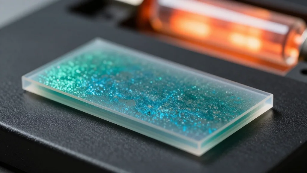
- •IISc achieved centimeter‑scale CrCl₃ films via low‑defect PVTD.
- •High carrier‑gas flow and darkened tube reduced imperfections.
- •Synthetic mica substrate yielded epitaxial, large‑grain growth.
- •Oxygen/moisture exclusion critical for preserving magnetic order.
- •Technique applicable to other air‑sensitive 2D materials.
Pulse Analysis
The allure of two‑dimensional magnetic crystals lies in their ability to retain spin ordering down to a single atomic layer, a property that promises ultra‑compact memory and sensor architectures. Yet, translating laboratory‑scale exfoliated flakes into manufacturable components has remained a bottleneck, primarily because conventional vapor‑phase techniques introduce lattice defects that quench magnetism. Researchers have long sought a growth platform that preserves the delicate exchange interactions while delivering uniform coverage across wafer‑sized substrates. Overcoming this hurdle would unlock a new class of spintronic devices that operate at lower power and higher speed than existing technologies.
The Indian Institute of Science team answered that call with a refined physical vapor transport deposition (PVTD) process. By darkening the growth tube and wrapping it in aluminum foil, stray radiative heat was minimized, while an unprecedented carrier‑gas flow swept vaporized chromium chloride across the chamber, promoting coalescence of crystalline domains. Real‑time control of material flux prevented over‑saturation, and a sealed, oxygen‑free environment eliminated oxidation that would otherwise destroy magnetic order. Synthetic mica emerged as the optimal substrate; its van‑der‑Waals surface acts as a lattice‑matched template, enabling epitaxial alignment and centimeter‑scale uniformity.
The breakthrough carries immediate commercial relevance. Wafer‑scale 2D magnetic films can be integrated directly into hard‑drive read heads, magnetic tunnel junctions, and on‑chip magnetic sensors, potentially shrinking device footprints and boosting energy efficiency. Moreover, the workflow is material‑agnostic: any air‑ or light‑sensitive 2D crystal could be grown using the same low‑defect protocol, expanding the library of functional layers for quantum computing, neuromorphic circuits, and flexible electronics. As the semiconductor industry pivots toward heterogeneous integration, this low‑defect PVTD method positions 2D magnetics as a viable component in next‑generation hardware roadmaps.
Wafer-scale 2D magnetic films emerge thanks to a new low-defect growth technique
Comments
Want to join the conversation?
Loading comments...