Atomic Moire Ferroelectrics Unlock Low Energy Nanoelectronics Potential
Key Takeaways
- •Moiré ferroelectrics exhibit switchable polarization at atomic scales
- •Stacking misaligned 2D layers creates novel electronic and optical properties
- •Fast polar response could outperform magnetic alternatives in memory devices
- •Research expands low‑energy nanoelectronics pathways beyond conventional materials
- •Findings open avenues for photonic components with tunable ferroelectric textures
Pulse Analysis
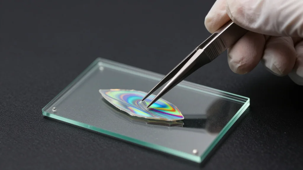
The concept of a moiré pattern—an interference fringe that appears when two periodic lattices are overlaid with a slight twist—has moved from optics into the realm of quantum materials. In van der Waals heterostructures, rotating atom‑thin layers creates superlattices whose electronic band structure can be tuned with sub‑nanometer precision. Recent work from Flinders University, Monash and Nanyang Technological University demonstrates that such engineered lattices can host ferroelectric order, a property traditionally limited to bulk oxides. This breakthrough expands the toolbox of 2‑D material engineering, enabling designers to embed switchable dipoles directly into a crystal lattice.
The emergence of switchable polarization at the atomic scale promises a new class of ultra‑low‑power devices. Ferroelectric dipoles can be toggled with millivolt‑level voltages, consuming orders of magnitude less energy than charge‑based transistors or spin‑torque magnetic memories. Moreover, the rapid response of these polar textures—often in the picosecond regime—makes them attractive for high‑density non‑volatile memory and neuromorphic computing where speed and energy efficiency are paramount. By integrating moiré ferroelectrics with existing silicon platforms, manufacturers could achieve dense, reconfigurable logic without the thermal penalties of conventional ferroelectric thin films.
Despite the promise, several hurdles remain before commercial adoption. Precise control of twist angle and interlayer spacing is required to reproducibly generate the desired ferroelectric domains, demanding advances in large‑scale stacking and in‑situ characterization. Stability of the polar state under ambient conditions and compatibility with standard CMOS processing also need validation. Nonetheless, the ability to engineer functional ferroelectricity without chemical doping could spur a wave of innovation across photonic modulators, energy‑harvesting sensors, and next‑generation memory architectures, positioning moiré ferroelectrics as a strategic research priority.
Atomic moire ferroelectrics unlock low energy nanoelectronics potential
Comments
Want to join the conversation?