Ballistic Electron Transport Observed in Single-Crystalline Copper Thin Films
Key Takeaways
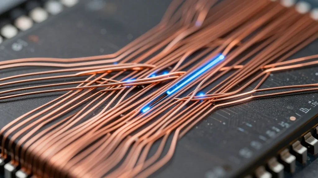
- •Ballistic transport observed in 80 nm Cu thin films
- •Single‑crystal Cu(111) grown via Atomic Sputtering Epitaxy
- •Negative bend resistance confirms scattering‑free electron flow
- •Potential to lower interconnect resistance and power consumption
Pulse Analysis
The discovery of ballistic electron transport in copper reshapes long‑standing assumptions about metal interconnects. Historically, ballistic behavior—where electrons traverse a conductor without scattering—has been confined to low‑dimensional quantum materials such as graphene or high‑mobility semiconductors. Copper’s strong electron‑phonon coupling and short mean free path made it a poor candidate, relegating it to diffusive transport regimes that increase resistive losses as dimensions shrink. By engineering a defect‑free, single‑crystal Cu(111) lattice with atomic‑scale smoothness, the research team eliminated grain boundaries and surface roughness, two primary scattering sources, thereby unlocking copper’s latent ballistic potential.
The experimental platform leveraged Atomic Sputtering Epitaxy to deposit 80 nm‑thick, 150 nm‑wide copper lines—sizes that mirror contemporary interconnect geometries. Nonlocal voltage measurements revealed a negative bend resistance signature, a hallmark of ballistic conduction, when the devices were cooled below 85 K. This temperature threshold aligns with reduced phonon activity, further extending the electron mean free path. The methodology demonstrates that, with precise crystallographic control, copper can transition from a conventional diffusive conductor to a quasi‑ballistic medium without resorting to exotic alloys or novel materials.
For the semiconductor ecosystem, the implications are profound. As Moore’s Law pushes feature sizes toward the sub‑100 nm regime, interconnect resistance becomes a dominant bottleneck, inflating signal delay and Joule heating. Ballistic copper interconnects promise to curb these effects, delivering lower latency and energy‑efficient operation—key attributes for high‑performance computing, AI accelerators, and mobile processors. While the current observations require cryogenic conditions, they establish a proof‑of‑concept that could inspire room‑temperature engineering through alloying, strain engineering, or advanced cooling strategies. Ultimately, integrating ballistic copper pathways may extend the scaling roadmap for silicon‑based technologies, preserving performance gains without abandoning the mature copper fabrication infrastructure.
Ballistic electron transport observed in single-crystalline copper thin films
Comments
Want to join the conversation?