Giant Second-Harmonic Generation Achieves 104 Susceptibility in Bismuth Monolayer
•February 2, 2026
0
Why It Matters
The discovery provides a scalable route to engineer 2D materials with record‑high nonlinear susceptibilities, opening pathways for compact quantum light sources and sub‑wavelength lasers. It also offers a direct optical signature for Dirac electrons in topological systems, accelerating material validation for photonic applications.
Key Takeaways
- •Buckling induces topological transition in bismuth monolayer.
- •SHG susceptibility exceeds MoS₂ by two orders magnitude.
- •Dirac cone formation adds another order of magnitude boost.
- •Susceptibility reaches ~10⁻⁶ m V⁻¹, highest for 2D ferroelectrics.
- •Tunable buckling enables on‑chip quantum light source design.
Pulse Analysis
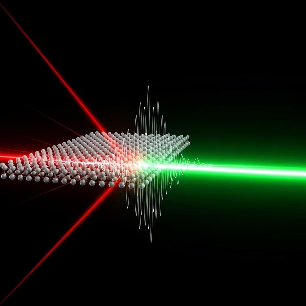
The breakthrough hinges on precise control of the bismuth monolayer’s out‑of‑plane buckling, which reshapes its electronic band topology. When the buckling height approaches 0.125 Å, a topological phase transition creates Dirac cones, concentrating low‑energy spectral weight and amplifying the second‑order susceptibility. First‑principles simulations reveal that this structural tuning not only narrows the band gap to ~0.27 eV but also aligns the ferroelectric polarization with C₂ᵥ symmetry, producing a synergistic boost in SHG that outperforms conventional transition‑metal dichalcogenides.
From a photonics perspective, such a giant χ^(2) enables highly efficient frequency‑doubling on a monolayer scale, dramatically reducing the power budget for on‑chip light‑frequency conversion. The material’s atomic thickness facilitates seamless integration with silicon photonic circuits and heterostructure engineering, allowing designers to embed nonlinear hotspots directly where they are needed. Moreover, the polarization‑resolved SHG signatures provide a straightforward diagnostic for device performance, making bismuth monolayers attractive for quantum light generation, entangled‑photon sources, and sub‑wavelength topological lasers that demand low‑threshold operation.
Looking ahead, experimental validation through strain‑engineered substrates or electrostatic gating could fine‑tune the buckling parameter, translating the theoretical gains into manufacturable components. Commercially, the ability to achieve order‑of‑magnitude higher SHG without resorting to bulky ferroelectric crystals promises a new class of compact, low‑cost nonlinear optical modules for telecommunications, sensing, and emerging quantum technologies. Continued collaboration between computational physicists and device engineers will be essential to bridge the gap from simulation to scalable production, positioning bismuth‑based 2D platforms at the forefront of next‑generation photonic integration.
Giant Second-Harmonic Generation Achieves 104 Susceptibility in Bismuth Monolayer
0
Comments
Want to join the conversation?
Loading comments...