Holes in Silicon Are Heavier than Expected - Solving a Mystery in Quantum Electronics
Key Takeaways
- •Holes in silicon have three times higher effective mass.
- •Measured electron mobility 40,000 cm²/V·s; hole mobility 2,000 cm²/V·s.
- •Mobility gap stems from intrinsic band structure, not defects.
- •Findings enable CMOS‑compatible hole‑based quantum devices.
- •Framework aids benchmarking cryogenic and space electronics.
Pulse Analysis
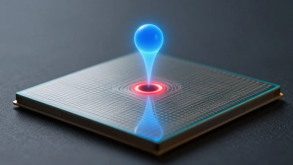
Silicon remains the workhorse of modern electronics, yet a long‑standing puzzle has been the stark contrast between electron and hole mobilities at cryogenic temperatures. While electrons zip through the crystal lattice with ease, holes crawl, limiting the performance of complementary circuits used in emerging quantum processors. Early theories blamed impurities or fabrication imperfections, but the new UNSW‑imec collaboration shows that the root cause lies in silicon’s band structure, where holes carry an effective mass roughly three times larger than previously assumed.
The research team leveraged state‑of‑the‑art 300 mm CMOS foundry processes and ultra‑cleanroom MOSFET fabrication to achieve record mobilities—40,000 cm² V⁻¹ s⁻¹ for electrons and 2,000 cm² V⁻¹ s⁻¹ for holes. By extending existing transport models, they linked the ten‑fold mobility gap directly to the heavier hole mass, eliminating defect‑related explanations. This refined understanding equips device engineers with a predictive framework for assessing interface quality, optimizing transistor geometry, and calibrating qubit designs without resorting to costly trial‑and‑error iterations.
Looking ahead, the insight that hole transport is fundamentally limited by mass rather than material flaws reshapes strategies for silicon‑based quantum hardware. It validates the feasibility of hole‑spin qubits and mixed‑carrier architectures built on standard CMOS lines, reducing development risk for cryogenic control electronics, space‑qualified sensors, and scalable quantum processors. As the community extends the model to isotopically enriched ^28Si and explores spin‑orbit coupling effects, the findings are set to accelerate Australia’s role in the global race for manufacturable quantum technologies.
Holes in silicon are heavier than expected - solving a mystery in quantum electronics
Comments
Want to join the conversation?