MXene Plasmonic Sensor Reveals Faint Molecular Fingerprints in Ultrathin Films
Key Takeaways
- •Acoustic MXene plasmons confine IR light within 10 nm gaps
- •Ti₃C₂Tₓ MXene enables broadband coverage up to short‑wave infrared
- •Device achieved up to 10× enhancement for faint polymer bands
- •Overlapping resonances provide ~5000 cm⁻¹ spectral bandwidth
- •Laboratory tests show stable performance after months of ambient storage
Pulse Analysis
Infrared spectroscopy is a cornerstone of chemical analysis, yet conventional sensors face a dilemma: they either cover a narrow spectral window with strong enhancement or provide broad coverage with insufficient sensitivity for ultrathin layers. The emergence of acoustic MXene plasmons reshapes this landscape. By exploiting the high carrier density of Ti₃C₂Tₓ, the resonator compresses infrared wavelengths more than a hundredfold, concentrating the optical field directly inside a nanometer‑scale analyte gap. This vertical confinement dramatically boosts interaction with molecular bonds, allowing detection of weak vibrational modes that would otherwise be lost in the noise.
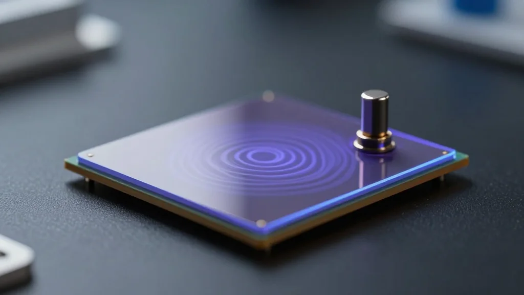
The AMP sensor’s architecture—gold nanodisks atop a sub‑10 nm MXene film on silicon—creates coupled acoustic plasmon modes whose resonance can be tuned via disk diameter. Unlike graphene‑based platforms limited to the mid‑infrared, Ti₃C₂Tₓ supports plasmonic activity well into the short‑wave infrared, delivering a continuous bandwidth of roughly 5000 cm⁻¹. Experimental validation with 8 nm PMMA and 10 nm graphene‑oxide films demonstrated up to ten‑fold signal amplification, revealing faint CH₃ combination bands near 4700 cm⁻¹ and oxygenated functional groups otherwise invisible to standard SEIRA setups.
For industry, this technology promises a single‑chip solution capable of rapid, non‑destructive analysis of ultra‑thin coatings, polymer residues, and two‑dimensional materials across a broad chemical spectrum. While the current work remains a laboratory proof‑of‑concept, its demonstrated stability under ambient storage and compatibility with existing nanofabrication processes suggest a viable path toward scalable manufacturing. Future efforts will likely focus on integrating microfluidic delivery, expanding multiplexed detection, and validating performance in real‑world environments such as semiconductor wafer inspection and environmental monitoring.
MXene plasmonic sensor reveals faint molecular fingerprints in ultrathin films
Comments
Want to join the conversation?