Researchers Pioneer Defect-Free High-Quality Graphene Electrodes
Key Takeaways
- •One‑step patterning creates sub‑5 µm graphene features
- •No photoresist or etching, preserving graphene integrity
- •Measured resistances: 11.5 Ω (5 µm) and 9.4 Ω (20 µm)
- •Process operates at 380 °C under 1,000 V vacuum
- •Enables clean electrodes for biosensors and flexible displays
Pulse Analysis
Transparent conductive electrodes are the linchpin of modern optoelectronic and bio‑electronic systems, yet traditional photolithography introduces contaminants and mechanical stress that erode graphene’s hallmark conductivity and flexibility. As manufacturers push toward thinner, more adaptable displays and implantable sensors, the industry has struggled to reconcile high‑resolution patterning with the need for pristine graphene surfaces. This tension has slowed the commercial rollout of graphene‑based components despite their superior optical transmittance and mechanical resilience.
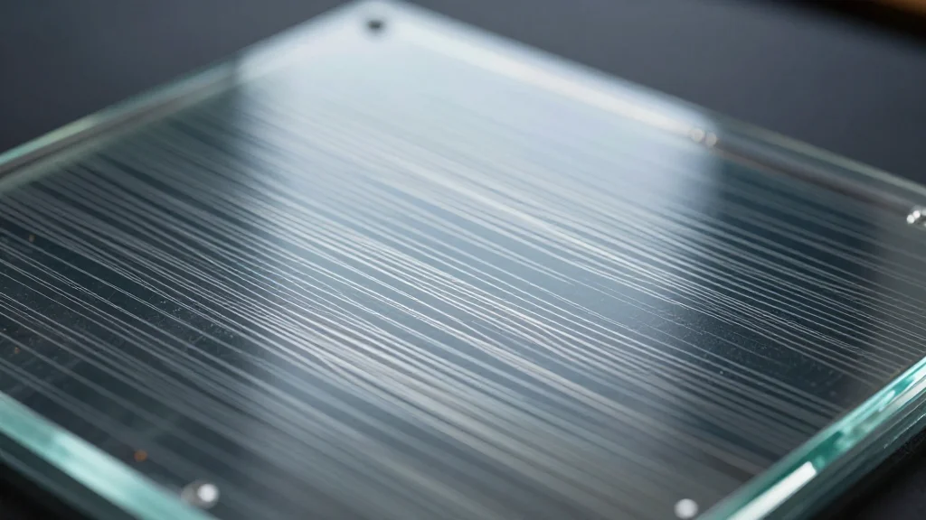
The newly reported one‑step free patterning of graphene (OFP‑G) sidesteps these obstacles by leveraging a solid‑electrolyte glass that becomes conductive under vacuum at 380 °C. When a 1,000 V bias is applied, alkali ions migrate, generating localized oxygen‑rich zones that selectively oxidize carbon bonds only where contact is made. This stencil‑like conversion yields sub‑5 µm features with resistances as low as 11.5 Ω, while the surrounding graphene remains untouched and free of polymer residues. Raman and XPS analyses confirm that the patterned regions retain structural integrity, delivering both high pattern fidelity and electrical performance.
The implications extend beyond laboratory proof‑of‑concept. A contamination‑free, scalable process aligns with the manufacturing realities of flexible displays, solar panels, and neural interfaces, where surface cleanliness directly impacts device reliability and biocompatibility. By eliminating costly photoresist steps and reducing defect‑induced yield losses, OFP‑G could lower production costs and accelerate time‑to‑market for graphene‑enabled products. As the sector seeks sustainable, high‑performance materials, this technique positions graphene as a viable mainstream contender for next‑generation transparent and wearable electronics.
Researchers pioneer defect-free high-quality graphene electrodes
Comments
Want to join the conversation?