Shows 76% of WSe2 Monolayer Sites Yield Stable Single-Photon Emitters Via AFM Nanoindentation
•February 4, 2026
0
Why It Matters
Deterministic, on‑chip quantum light sources bridge 2D materials and silicon photonic platforms, accelerating scalable quantum communication and computing hardware.
Key Takeaways
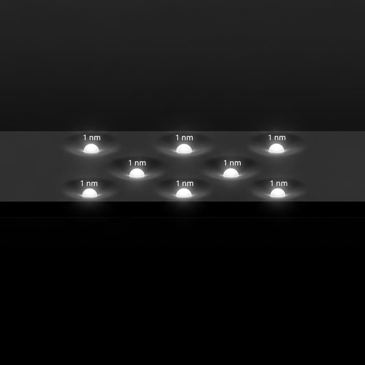
- •AFM nano‑indentation >150 nm creates WSe₂ single‑photon emitters
- •Emitters show ≈200 µeV linewidths, stable to ~120 K
- •g²(0) < 0.5 confirms true single‑photon behavior
- •Electrical gating enables on/off switching of emitters
- •Yield 0.76% per indentation, deterministic placement achieved
Pulse Analysis
Two‑dimensional semiconductors have long promised compact quantum emitters, yet most strain‑engineered approaches rely on random defect formation or complex nanopillar arrays that are difficult to align with existing silicon photonic circuitry. The AFM nano‑indentation method sidesteps these limitations by using a rigid 350 N m⁻¹ cantilever and precise Z‑piezo displacement, delivering repeatable sub‑nanometer control over strain fields directly on SiO₂/Si wafers. This deterministic process not only simplifies fabrication but also opens a clear pathway for integrating 2D quantum emitters into mature CMOS‑compatible platforms.
Beyond placement accuracy, the optical performance of the WSe₂ emitters rivals that of epitaxial quantum dots. Linewidths as narrow as 200 µeV and thermal stability up to 120 K indicate low phonon coupling and robust confinement, while g²(0) values below 0.5 verify true single‑photon statistics. The addition of a back‑gate allows researchers to modulate carrier populations, suppress background photoluminescence, and fine‑tune emission dynamics, offering a level of electrical control rarely achieved in 2D‑based quantum light sources. Such capabilities are critical for on‑chip quantum repeaters and entanglement distribution networks.
Looking ahead, the technique’s compatibility with other transition‑metal dichalcogenides and ferroelectric substrates suggests a versatile toolkit for engineering a spectrum of quantum emitters, including chiral and spin‑valley variants. Coupling these deterministic sites to high‑Q photonic crystal cavities or waveguides could dramatically boost emission rates via Purcell enhancement, paving the way for scalable quantum photonic processors. As the industry seeks turnkey quantum light modules, this AFM‑driven approach positions 2D materials as a practical bridge between laboratory breakthroughs and commercial quantum technologies.
Shows 76% of WSe2 Monolayer Sites Yield Stable Single-Photon Emitters Via AFM Nanoindentation
0
Comments
Want to join the conversation?
Loading comments...