Stacked Atom Thin Materials Enable a New Form of Ultralow Power Memory
Key Takeaways
- •Graphene/hBN/α‑RuCl₃ stack creates artificial ferroelectricity
- •Memory operates at −243 °C with five‑month retention
- •Electrical switching independent of magnetic fields
- •Potential for ultralow‑power quantum‑computer memory
- •Eliminates thickness limits of conventional ferroelectrics
Pulse Analysis
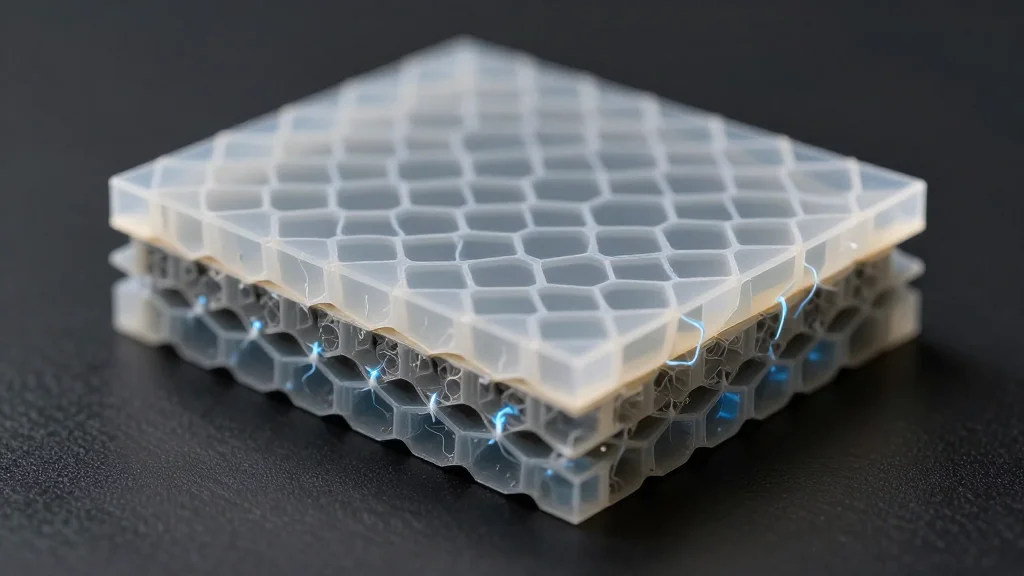
The race for ever‑smaller, energy‑efficient memory has long been hampered by the physics of traditional ferroelectric materials, which lose their polarization as they are thinned below a few nanometres. Engineers have therefore explored alternative mechanisms, from phase‑change alloys to spin‑based storage, yet each brings trade‑offs in power consumption, scalability, or fabrication complexity. The recent discovery that a simple van‑der‑Waals stack of graphene, hBN, and α‑RuCl₃ can spontaneously generate interfacial dipoles sidesteps these hurdles, delivering ferroelectric‑like behavior without the need for bulk ferroelectric crystals or strain engineering.
In the reported heterostructure, an atom‑thin insulating hBN layer separates conductive graphene from the magnetic insulator α‑RuCl₃. Charge redistribution at the two interfaces creates a bistable electric dipole that can be toggled with modest voltage pulses, effectively writing and erasing bits. Remarkably, the device remains stable at –243 °C (30 K) and retains its state for more than five months without power, demonstrating true non‑volatility at cryogenic temperatures. Because the switching relies solely on electric fields, it is immune to external magnetic disturbances, simplifying system design for environments where magnetic noise is a concern.
The implications extend beyond academic curiosity. Quantum processors operate at millikelvin temperatures and demand memory that adds negligible thermal load; a graphene‑based ultralow‑power cell fits that niche. Moreover, the stack’s planar, wafer‑compatible architecture aligns with existing semiconductor manufacturing, promising a smoother transition to commercial products. As the industry pushes toward thinner, lighter consumer electronics and energy‑constrained edge devices, this stacking strategy could become a cornerstone for next‑generation non‑volatile memory, marrying scalability with the ultra‑low power budgets of future computing platforms.
Stacked atom thin materials enable a new form of ultralow power memory
Comments
Want to join the conversation?