Stacking 2D Materials on Bulk Semiconductors Yields Smarter, Faster Photodetectors
Key Takeaways
- •Van der Waals bonding enables defect‑free 2D/3D stacking
- •Devices achieve >1000 A/W responsivity and 10¹³ Jones detectivity
- •Interface traps create on‑chip synaptic behavior, cutting AI vision power
- •Band‑structure and geometry engineering boost speed to gigahertz range
- •Wafer‑scale 2D growth and stability remain manufacturing hurdles
Pulse Analysis
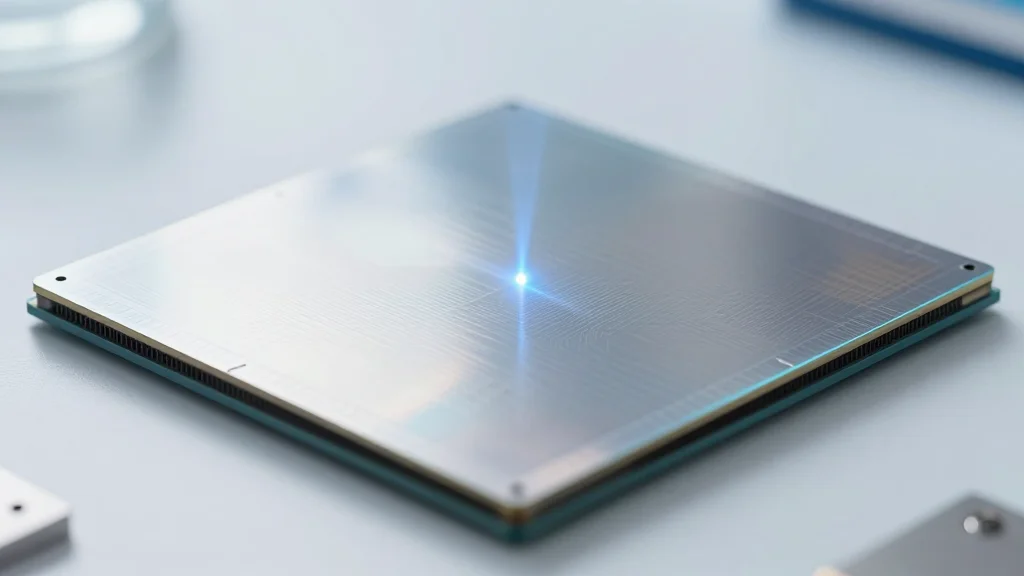
Traditional photodetectors built on bulk silicon, germanium or III‑V compounds face inherent trade‑offs: fixed spectral windows, high dark current and costly lattice‑matched epitaxy. By leveraging the weak van der Waals forces that bind 2D crystals to any substrate, engineers can bypass these constraints and assemble heterostructures with atomically clean interfaces. This flexibility lets a single chip combine the thick, high‑absorption 3D layer with a tunable, ultra‑fast 2D surface, extending detection from visible light into the mid‑infrared while suppressing noise sources that limit sensitivity.
The review highlights four engineering levers that have pushed performance to the brink of commercial viability. Band‑structure alignment (type‑II or type‑III) directs carriers into separate layers, minimizing recombination, while ultra‑thin insulating interlayers filter out low‑energy dark carriers. Electrical gating of the 2D sheet enables real‑time reconfiguration between sensing and logic modes, and textured 3D substrates such as nanocones increase photon trapping and strain‑tune the 2D bandgap. These tactics collectively deliver responsivities above 1000 A/W and detectivities of 10¹³ Jones—metrics once reserved for cryogenically cooled infrared detectors—plus gigahertz response speeds suitable for 6G optical links.
Beyond raw numbers, the integration of charge‑trapping synaptic behavior transforms the detector into a front‑end processor, slashing the 80‑90 % power overhead of conventional AI vision pipelines. This in‑sensor computing can pre‑filter, denoise and even recognize patterns before data leaves the chip, a game‑changer for low‑power autonomous robots and edge‑AI cameras. However, scaling remains a hurdle: uniform 2D film growth on 12‑inch wafers and robust encapsulation of air‑sensitive materials like black phosphorus are still under development. As CMOS‑compatible fabrication matures, 2D/3D van der Waals photodetectors are poised to power next‑generation hyperspectral imaging, smart‑phone cameras and ultra‑efficient machine‑vision systems.
Stacking 2D materials on bulk semiconductors yields smarter, faster photodetectors
Comments
Want to join the conversation?