Key Takeaways
- •Argon flux tuning controls ammonia‑borane decomposition, improving h‑BN film quality
- •Optimized films exhibit room‑temperature single‑photon emission, essential for quantum devices
- •Atmospheric‑pressure CVD enables large‑area h‑BN growth without complex chemistries
- •Scalable defect engineering paves way for commercial quantum photonic circuits
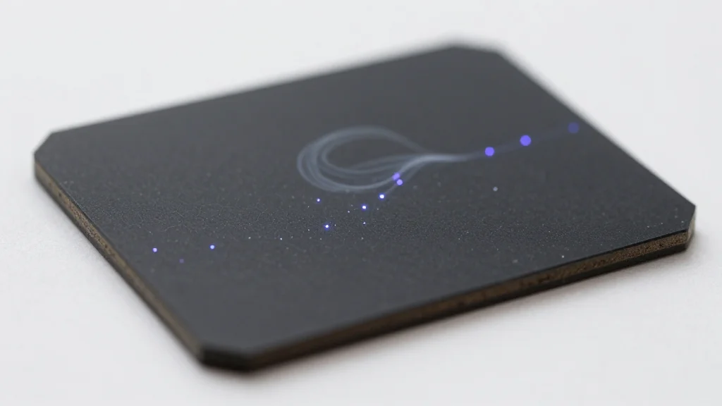
Pulse Analysis
Hexagonal boron nitride (h‑BN) has emerged as a versatile two‑dimensional platform because of its wide band gap, chemical inertness, and ability to host point defects that act as quantum emitters. Unlike graphene, h‑BN does not conduct electricity, making it ideal for optoelectronic applications where isolated photon generation is required. The material’s honeycomb lattice, slightly expanded relative to graphene, supports stable defect centers that can emit one photon at a time—a prerequisite for quantum key distribution and high‑resolution sensing.
The new growth protocol leverages atmospheric‑pressure chemical vapor deposition (AP‑CVD) and focuses on the decomposition dynamics of ammonia‑borane, the precursor for boron and nitrogen atoms. By systematically varying argon gas flow, the researchers modulated the thermal environment, influencing defect density and crystal uniformity. This subtle adjustment produced h‑BN films with consistent structural quality and, crucially, reproducible single‑photon emitters that operate at ambient conditions. The approach sidesteps the need for elaborate post‑growth treatments or exotic dopants, offering a more straightforward path to large‑scale production.
From a market perspective, scalable h‑BN single‑photon sources could lower the barrier to entry for quantum photonic circuits, enabling manufacturers to integrate quantum light sources directly onto chips. This aligns with industry trends toward on‑chip quantum communication and sensing solutions, where cost‑effective, room‑temperature operation is a decisive advantage. As the quantum ecosystem matures, the ability to reliably produce defect‑engineered h‑BN at wafer scale may drive new business models, from secure networking hardware to advanced metrology devices, positioning the technology as a cornerstone of next‑generation quantum infrastructure.
Tuning 2D materials growth for quantum photonics
Comments
Want to join the conversation?