Twist-Angle Engineering Boosts Perovskite Optoelectronic Performance
Key Takeaways
- •15° twist yields 2.8 A W⁻¹ responsivity, 2.33×10⁵ on/off ratio
- •Interlayer coupling strengthens monotonically with twist angle
- •Bandgap narrows, enhancing carrier transport and mobility
- •Technique works despite perovskite’s soft lattice and strong phonon coupling
Pulse Analysis
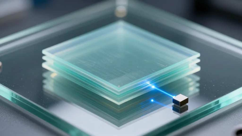
Twistronics, the practice of rotating stacked two‑dimensional crystals to tailor electronic properties, has reshaped condensed‑matter research since the discovery of superconductivity in twisted bilayer graphene. While most successes have involved rigid, inorganic lattices, soft organic‑inorganic perovskites were long considered unsuitable because their flexible frameworks and strong electron‑phonon interactions could obscure angle‑dependent effects. The new study overturns this assumption by systematically varying the twist angle between (PEA)₂PbBr₄ and monolayer WSe₂, demonstrating that even pliable perovskite layers respond predictably to rotational tuning.
The researchers fabricated six heterojunctions from 0° to 15° and observed a steady increase in interlayer coupling, evidenced by phonon hardening and red‑shifted photoluminescence. Density‑functional theory revealed a continuous bandgap reduction and reinforced type‑II band alignment, which together improve charge separation and carrier mobility. Device measurements mirrored these trends: the 15° stack delivered a record‑high responsivity of 2.8 A W⁻¹ under 405 nm illumination, an on/off ratio exceeding 200,000, and hole mobility above 117 cm² V⁻¹ s⁻¹—metrics that surpass prior perovskite/TMD photodetectors.
By proving that twist angle can serve as a universal, composition‑agnostic lever for performance optimization, the work opens a pathway for rapid prototyping of ultrathin optoelectronic components such as photodetectors, light‑emitters, and flexible sensors. Industry players can now explore perovskite‑based devices without redesigning chemistry for each target application, potentially shortening development cycles and reducing material costs. Future research will likely focus on scaling the technique to larger wafer formats, integrating additional 2D partners, and exploiting the tunable bandstructure for broadband detection and energy‑harvesting technologies.
Twist-angle engineering boosts perovskite optoelectronic performance
Comments
Want to join the conversation?