Ultrafast Diamond Sensor Achieves 10-Fs Electric Field Detection
•January 26, 2026
0
Why It Matters
The sensor breaks diffraction‑limited constraints, enabling real‑time electric‑field mapping of nanodevices, which is critical for advancing quantum electronics and ultrafast material diagnostics.
Key Takeaways
- •Diamond NV tip achieves ≤500 nm spatial resolution
- •Temporal resolution reaches ≤100 fs using 10 fs pulses
- •Pockels effect enabled via NV‑induced second‑order susceptibility
- •Nanoscale EO mapping demonstrated on n‑GaAs surface
- •Signal amplitude reduced to 1/42 compared with macroscopic measurements
Pulse Analysis
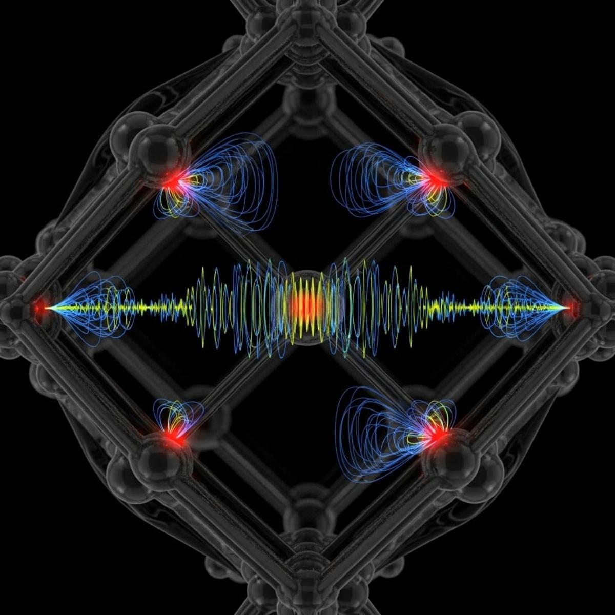
Traditional electro‑optic sensors rely on bulk ferroelectric crystals and are limited by the diffraction of light, restricting spatial resolution to the micrometer scale. Diamond’s nitrogen‑vacancy centres provide a quantum‑grade platform that combines optical addressability with a non‑zero second‑order susceptibility, allowing the Pockels effect to be harnessed at the nanoscale. By embedding NV defects just 40 nm beneath the diamond surface, the researchers created a probe that responds to local electric fields without the need for external microwave driving, sidestepping the complexity of conventional NV‑spin readout schemes.
The experimental setup merges an ultrashort Ti:sapphire laser (≤10 fs pulses spanning 660–940 nm) with a reflective Schwarzschild objective to minimize dispersion, and couples this to an atomic‑force‑microscopy cantilever. This hybrid pump‑probe‑SPM system delivers a combined spatial‑temporal resolution of ≤500 nm and ≤100 fs, respectively. When tested on n‑type GaAs, the sensor recorded a field change of roughly –3.1 × 10⁶ V m⁻¹ and a 0.5 ps relaxation, confirming its ability to capture fast carrier dynamics in a sub‑micron probing area. The observed 1/42 reduction in signal amplitude relative to macroscopic measurements aligns with the smaller interaction volume and heightened surface scattering.
The breakthrough paves the way for high‑resolution electro‑optic characterization of emerging nanomaterials, two‑dimensional semiconductors, and quantum devices where electric‑field transients dictate performance. Industries ranging from semiconductor manufacturing to photonic integrated circuits can leverage this capability to diagnose device failures, optimize carrier transport, and explore novel quantum phenomena. As the technique matures, integration with on‑chip photonics and scalable diamond fabrication could transform ultrafast metrology into a standard tool for next‑generation electronics.
Ultrafast Diamond Sensor Achieves 10-Fs Electric Field Detection
0
Comments
Want to join the conversation?
Loading comments...