A CMOS-Compatible, Scalable and Compact Magnetoelectric Spin-Torque Microwave Detector
•March 2, 2026
0
Why It Matters
The breakthrough enables on‑chip, high‑sensitivity microwave detection for IoT, radar and communications, reducing system size and power consumption while leveraging existing CMOS fabs.
Key Takeaways
- •Integrated ME antenna and MTJ yields >90 kV W⁻¹ sensitivity.
- •Noise equivalent power reaches 3 pW Hz⁻¹/².
- •Device footprint only 0.4 mm², CMOS‑compatible.
- •Four‑MTJ array boosts sensitivity beyond 400 kV W⁻¹.
- •Scalable design enables on‑chip microwave detection for IoT.
Pulse Analysis
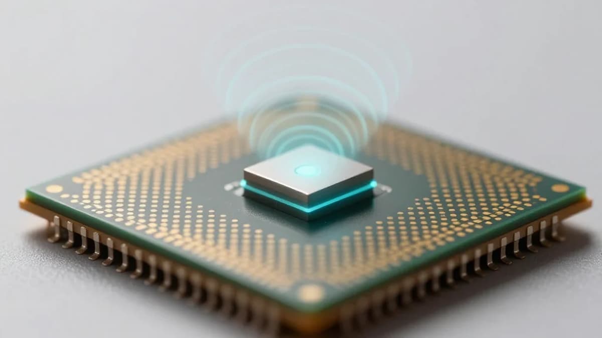
Spin‑torque diodes have long promised microwave detection beyond the thermodynamic limits of conventional Schottky diodes, yet their adoption has been hampered by bulky external antennas and incompatibility with standard silicon processes. By embedding a magnetoelectric (ME) antenna directly on a magnetic tunnel junction (MTJ), the new detector sidesteps these constraints, delivering a fully monolithic solution that can be fabricated alongside CMOS circuitry. This integration leverages strain‑mediated magnetoelectric coupling to translate incident RF fields into voltage across the MTJ, where spin‑transfer torque rectifies the signal, producing a DC output without the need for ancillary components.
The reported performance metrics are striking: a sensitivity greater than 90 kV W⁻¹ and a noise‑equivalent power of 3 pW Hz⁻¹/² place the device well ahead of typical semiconductor diodes, while its 0.4 mm² footprint meets the stringent area budgets of modern chips. Moreover, the architecture scales gracefully; an array of four MTJs raises sensitivity beyond 400 kV W⁻¹, illustrating a clear path toward higher‑gain, multi‑pixel detectors without sacrificing CMOS compatibility. Such scalability is crucial for applications that demand both high dynamic range and spatial resolution, such as phased‑array radar and on‑chip spectrum sensing.
For the broader industry, this technology could accelerate the rollout of ultra‑compact microwave front‑ends in 5G/6G infrastructure, autonomous‑vehicle radar, and low‑power IoT nodes that harvest ambient RF energy. The ability to fabricate these detectors in existing foundries reduces development cost and shortens time‑to‑market, while the magnetoelectric approach opens new avenues for energy‑efficient signal processing. As the ecosystem moves toward heterogeneous integration, magnetoelectric spin‑torque detectors are poised to become a cornerstone of next‑generation wireless and sensing platforms.
A CMOS-compatible, scalable and compact magnetoelectric spin-torque microwave detector
0
Comments
Want to join the conversation?
Loading comments...