A New Microscope for the Quantum Age: Single Nanoscale Scan Measures Four Key Material Properties
•February 12, 2026
0
Why It Matters
By delivering simultaneous multimodal imaging, the microscope removes a major bottleneck in quantum material characterization and enables fast fault detection in quantum chips, crucial for scaling quantum technologies.
Key Takeaways
- •Simultaneous temperature, magnetic, structural, electrical mapping at nanoscale
- •Works on uneven quantum chips, not just flat samples
- •Enables rapid diagnostics for failing quantum computing components
- •Developed by Leiden team, commercialized by QuantaMap
- •Reduces experimental bottlenecks in quantum material research
Pulse Analysis
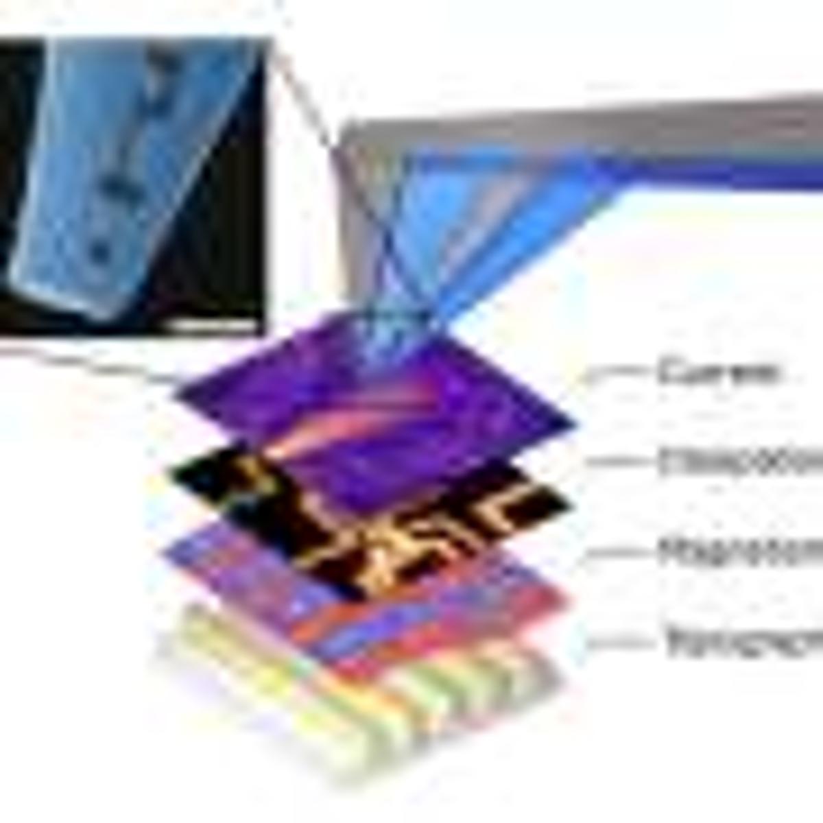
The emergence of multimodal quantum microscopy marks a turning point for materials science, where researchers have long struggled to correlate thermal, magnetic, structural, and electronic phenomena that coexist at the nanometer scale. Traditional techniques require separate instruments, each with its own alignment and calibration challenges, slowing discovery cycles. By integrating a SQUID‑on‑Tip sensor with tapping‑mode operation, the new microscope captures four critical parameters in a single pass, preserving spatial fidelity and dramatically cutting measurement time. This capability is especially valuable for probing quantum materials whose properties are intrinsically intertwined, such as high‑temperature superconductors and topological insulators.
From a technical perspective, the TM‑SOT design leverages proximity Josephson junctions to achieve unprecedented sensitivity while maintaining a robust tip that tolerates surface roughness. Unlike conventional scanning probe microscopes that demand atomically flat substrates, the Leiden system can scan bumpy quantum chips, revealing edge effects and interface phenomena that were previously inaccessible. The instrument’s modular construction—born from a blend of repurposed parts and custom‑engineered components—demonstrates a pragmatic approach to high‑performance instrumentation, paving the way for broader adoption in university labs and industry R&D centers.
Commercially, QuantaMap’s effort to bring the microscope to market addresses a critical void in quantum‑hardware diagnostics. As quantum processors scale up, yield loss due to undetected defects becomes a costly barrier. Real‑time, nanoscale diagnostics enable manufacturers to pinpoint failure modes, refine fabrication processes, and accelerate time‑to‑market for quantum computers. Moreover, the technology’s versatility opens opportunities in quantum sensing, cryogenic electronics, and next‑generation metrology, positioning it as a foundational tool for the quantum age.
A new microscope for the quantum age: Single nanoscale scan measures four key material properties
0
Comments
Want to join the conversation?
Loading comments...