A New, Useful Absorption Limit for Ultra-Thin Films
•February 26, 2026
0
Why It Matters
Breaking the 50% absorption barrier dramatically improves the performance ceiling for graphene‑based optics and other ultrathin photonic components, reshaping design strategies in terahertz and infrared technologies.
Key Takeaways
- •Absorption reaches 82.8% at grazing incidence for ultrathin films
- •Traditional 50% limit broken by high conductivity at grazing angles
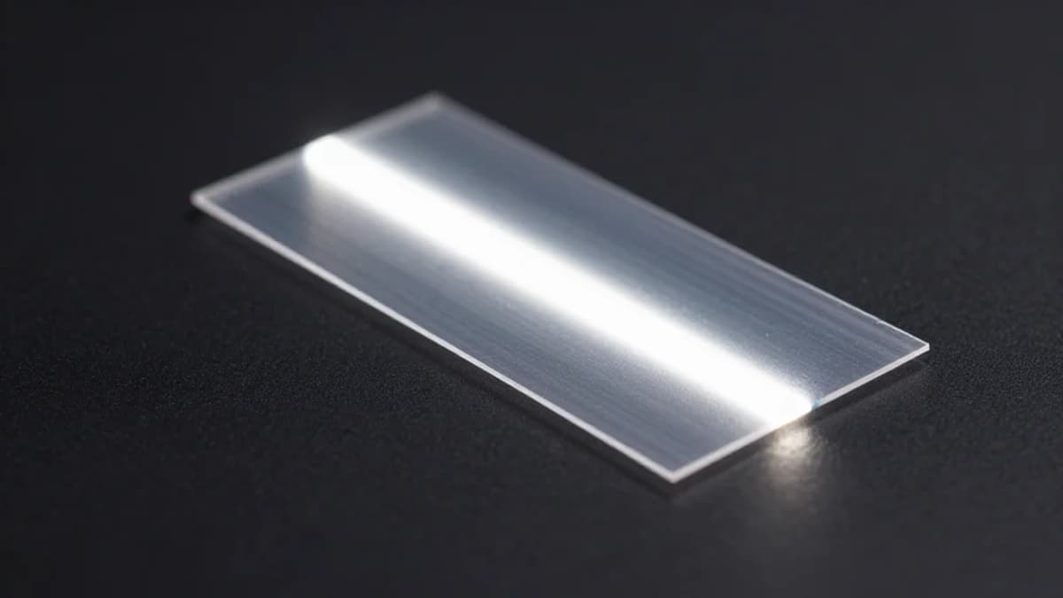
- •Experiment with 10‑µm silicone film confirms theoretical prediction
- •Effect holds for terahertz, microwave, infrared, and noble metals
- •Enables efficient terahertz modulators and wide‑angle photodetectors
Pulse Analysis
The optics community has long accepted that atom‑scale conductors such as graphene can at best capture half of the incoming photons, a rule derived from symmetric electric‑field arguments. That constraint has limited the ambition of designers seeking ultra‑lightweight, transparent electrodes for flexible displays, solar cells, and high‑speed sensors. By revisiting the boundary conditions for transverse‑magnetic (TM) waves at extreme angles, the new study overturns this dogma, showing that the thin‑film’s effective conductivity spikes when the wave grazes the surface, allowing far greater energy dissipation.
The authors employed a rigorous Maxwell‑equation framework to predict a universal absorption ceiling of 2√2 − 2, or roughly 82.8%, for any film whose thickness is negligible compared with the wavelength. Laboratory measurements with a 10‑micron conductive silicone sheet, illuminated at terahertz frequencies, tracked the absorption curve up to 80° incidence and matched the theoretical peak. Parallel tests with microwaves, infrared light, and even noble‑metal layers reproduced the same enhancement, confirming that the phenomenon is material‑agnostic and driven primarily by geometry and polarization.
From a commercial perspective, the breakthrough unlocks design space for devices that must remain thin yet highly absorptive. Terahertz modulators can now achieve stronger modulation depth without bulky absorbers, while photodetectors can capture light over a wider angular range, improving sensitivity in imaging and sensing platforms. Moreover, the principle extends to emerging 2‑D materials like MXenes, suggesting a broader class of ultra‑thin components that can be engineered for maximal light‑matter interaction. Future work will likely focus on scalable fabrication techniques to maintain precise grazing‑angle alignment and on integrating these films into next‑generation optoelectronic circuits.
A new, useful absorption limit for ultra-thin films
0
Comments
Want to join the conversation?
Loading comments...