A Wafer-Scale Optoelectronic Device Unlocks Monolithic 3D Integration
•February 25, 2026
0
Why It Matters
The ability to fabricate wafer‑scale anisotropic boridene with BEOL compatibility accelerates the integration of optoelectronic functions into existing semiconductor fabs, reshaping AI‑hardware roadmaps. It promises higher performance and lower power for next‑generation computing platforms.
Key Takeaways
- •Ordered vacancies create anisotropic electrical behavior.
- •Enables bipolar and linear photocurrent for computing.
- •Low-temperature deposition suits back‑end‑of‑line processes.
- •Scalable 12‑inch wafer arrays support monolithic 3D integration.
- •Potential to accelerate optoelectronic AI hardware.
Pulse Analysis
The recent demonstration of electrically anisotropic boridene marks a pivotal advance in two‑dimensional (2D) material engineering. By deliberately introducing ordered vacancies into the (Mo₂/₃Y₁/₃)₂AlB₂ lattice, researchers have induced a pronounced directional conductivity that produces both bipolar and linear photocurrents under illumination. This anisotropy directly addresses a long‑standing bottleneck in optoelectronic computing, where symmetric charge transport limits signal modulation speed and energy efficiency. The material’s intrinsic band structure, combined with vacancy‑driven polarity, enables programmable photonic logic without additional doping steps. These findings also suggest a new design paradigm for future photonic circuits.
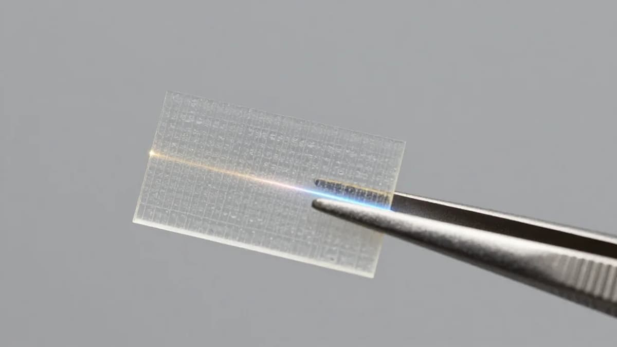
Beyond its electronic merits, the boridene platform is designed for back‑end‑of‑line (BEOL) integration, leveraging a low‑temperature deposition process compatible with existing 200 mm and 300 mm silicon lines. The heterojunction architecture can be patterned across a full 12‑inch wafer, delivering uniform device performance without the thermal budgets that typically damage underlying circuits. Such scalability bridges the gap between laboratory‑scale 2D prototypes and mass‑production, allowing semiconductor manufacturers to embed optoelectronic layers directly onto mature CMOS stacks. This approach reduces interconnect length and opens pathways for true monolithic 3D stacking. The process also demonstrates compatibility with standard photoresist chemistries, simplifying integration.
For the broader semiconductor market, wafer‑scale anisotropic boridene could accelerate the rollout of AI‑focused accelerators that rely on photonic‑electronic hybrid computing. The ability to generate linear photocurrents at low power promises higher throughput for vision sensors, edge inference, and neuromorphic processors. Moreover, monolithic 3D integration minimizes latency and footprint compared with traditional chip‑on‑wafer or package‑on‑package solutions. As industry players seek to overcome the end of Moore’s Law, this technology offers a viable route to increase functional density while maintaining compatibility with current fab infrastructure. Early adoption could position early movers as leaders in next‑generation compute platforms.
A wafer-scale optoelectronic device unlocks monolithic 3D integration
0
Comments
Want to join the conversation?
Loading comments...