AI-Guided Electron Microscope Provides Unique Glimpse Into the World of MXenes
Why It Matters
The ability to visualize and control atomic‑scale defects unlocks precise tuning of MXene properties, a key step toward commercializing high‑performance batteries and filtration membranes. This breakthrough also establishes a new workflow for AI‑enhanced microscopy across advanced materials.
Key Takeaways
- •AI-driven microscopy reconstructs 3D defect topology in MXenes
- •First 3D visualization of titanium vacancies in 2‑D MXene layers
- •Defect mapping reveals impact on electrical and chemical reactivity
- •Enables targeted engineering of MXenes for batteries and water purification
- •Collaboration includes NLR, Purdue, Argonne, Colorado Mines, Baylor, CU Boulder
Pulse Analysis
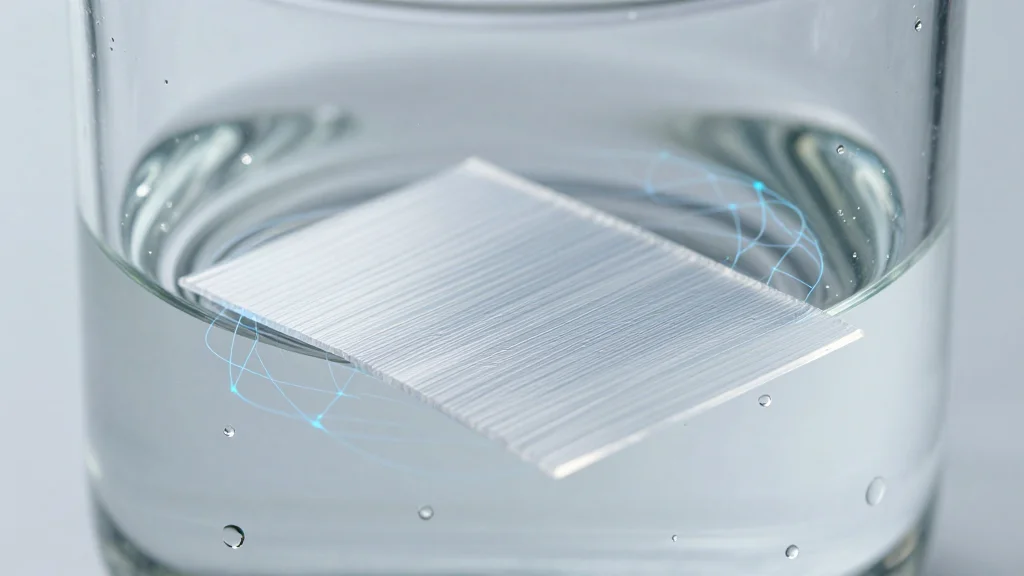
MXenes—ultrathin sheets of transition‑metal carbides and nitrides—have attracted intense interest for next‑generation batteries, water‑purification membranes, and flexible electronics. Their performance hinges on atomic‑scale imperfections, yet traditional electron microscopy could only capture defects in two dimensions, leaving a critical knowledge gap about how vacancies and distortions propagate through the material’s depth. Overcoming this limitation required a method that could translate a series of 2D projections into a coherent three‑dimensional picture, a challenge that has now been met through the fusion of high‑resolution microscopy and artificial intelligence.
The breakthrough stems from an AI‑guided electron microscope that employs machine‑learning algorithms to de‑convolute raw imaging data and reconstruct the full lattice of a titanium‑carbon MXene layer by layer. By training the model on known atomic configurations, the system identifies missing atoms—primarily titanium vacancies—and assigns them to specific planes within the sheet. This 3D defect topology not only quantifies vacancy concentration per layer but also reveals how defects migrate toward surfaces, altering reactivity and conductivity. Such granular insight enables scientists to predict how engineered defect patterns will affect charge transport, thermal management, and chemical stability, turning what was once a stochastic variable into a design parameter.
For industry, the ability to map and manipulate defects opens a pathway to scale MXene production with predictable performance metrics. Battery manufacturers can now tailor vacancy distributions to boost ion diffusion rates, while water‑treatment firms can engineer surface defects that enhance contaminant adsorption. The collaborative effort—spanning NLR, Purdue, Argonne, Colorado School of Mines, Baylor, and CU Boulder—demonstrates a model for interdisciplinary research that accelerates material innovation. As AI‑enhanced microscopy matures, it is poised to become a standard tool in the rapid prototyping of advanced 2D materials, shortening development cycles and reducing reliance on costly trial‑and‑error experiments.
AI-guided electron microscope provides unique glimpse into the world of MXenes
Comments
Want to join the conversation?
Loading comments...