Applied Materials Launches Two Deposition Tools for Sub‑2 Nm GAA Transistor Production
Companies Mentioned
Why It Matters
The two deposition tools address the most pressing bottleneck in sub‑2 nm GAA manufacturing: achieving atomic‑scale precision across a massive number of process steps. By improving isolation and gate‑stack uniformity, the equipment can lift performance per watt, a critical metric for AI accelerators that consume large amounts of power. Successful adoption will also validate materials‑driven scaling as a viable path beyond the limits of conventional lithography, influencing the strategic roadmaps of major foundries and chip designers. Beyond immediate performance gains, the launch signals a broader shift toward integrated, multi‑function deposition platforms. Consolidating several metal steps onto a single ALD system reduces fab floor space and cycle time, potentially lowering the total cost of ownership for advanced nodes. This could accelerate the rollout of AI‑centric chips, reinforcing the feedback loop between semiconductor capability and AI workload growth.
Key Takeaways
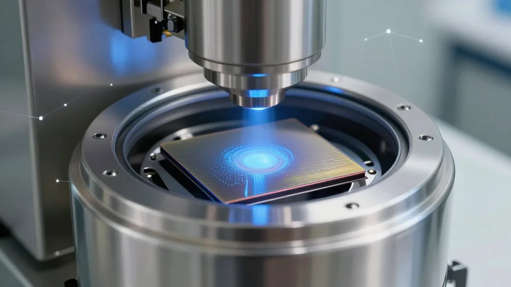
- •Applied Materials introduced a selective silicon nitride PECVD and an ALD system for sub‑2 nm GAA transistors.
- •GAA fabrication requires more than 500 process steps with near‑atomic tolerances.
- •The PECVD tool reduces parasitic capacitance by coating STI structures with silicon nitride.
- •The ALD platform integrates multiple metal deposition steps, enabling per‑transistor threshold tuning.
- •Pilot production slated for late 2026, with full rollout expected in 2027.
Pulse Analysis
Applied Materials' dual‑tool launch arrives at a juncture where traditional scaling is hitting physical limits. By focusing on materials engineering rather than lithography alone, the company is betting that precision deposition will become the new lever for performance gains. This strategy mirrors the broader industry pivot toward "materials‑first" roadmaps, where innovations in deposition, etch, and metrology drive node advancement.
Historically, each new deposition technology has unlocked a generation of chips— from high‑k metal gates to extreme ultraviolet (EUV) lithography. The selective silicon nitride PECVD and the integrated ALD system could be the next inflection point, especially for AI workloads that demand both high compute density and energy efficiency. Foundries that adopt these tools early may secure a competitive edge, offering customers chips that deliver more FLOPs per watt, a decisive factor in data‑center economics.
Looking ahead, the success of these systems will hinge on how quickly customers can integrate them into existing fab lines without disrupting throughput. If pilot runs demonstrate the promised yield improvements and cycle‑time reductions, we can expect a cascade of investments in GAA‑centric fabs, further entrenching AI as the primary driver of semiconductor innovation. Conversely, any delays or performance shortfalls could reinforce skepticism about materials‑centric scaling, prompting a re‑evaluation of alternative approaches such as 3D stacking or heterogeneous integration.
Applied Materials launches two deposition tools for sub‑2 nm GAA transistor production
Comments
Want to join the conversation?
Loading comments...